
New Imaging Technology with High Sensitivity for High Speed Analysis
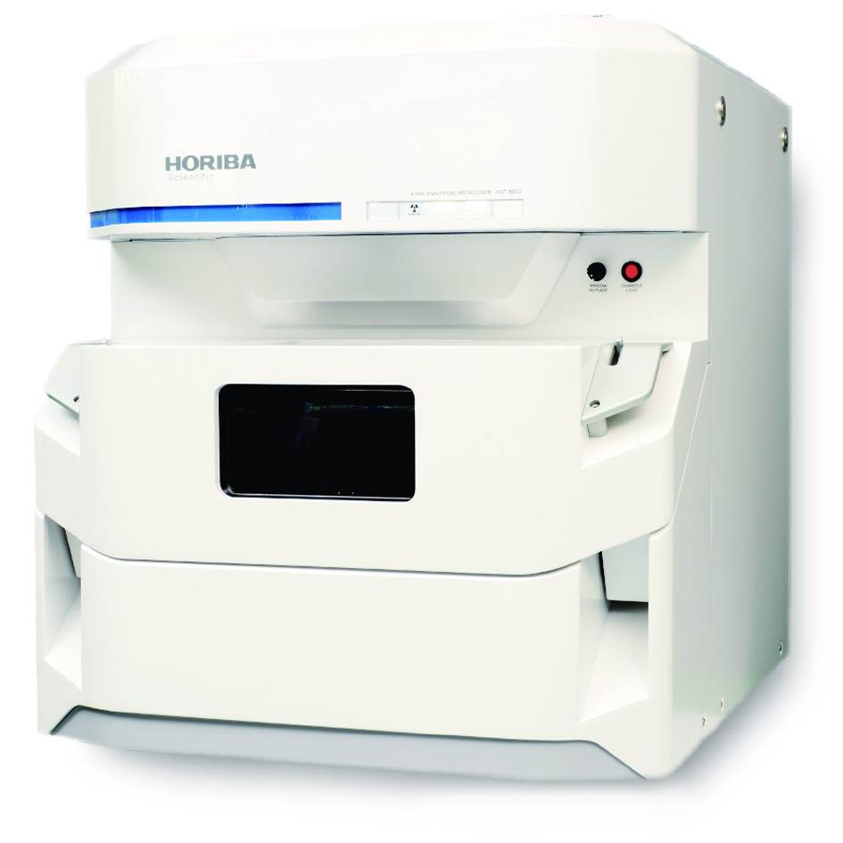
HORIBA Scientific, a global supplier of spectroscopy instrumentation and solutions, announces the release of its new XGT-9000 X-ray analytical microscope (μXRF), which simultaneously performs elemental analysis and optical observation of samples without destroying or contacting them. Incorporating HORIBA’s proprietary X-ray technology, with the highest resolution in the world, the XGT-9000 not only screens foreign objects that often cause problems in the production process of lithium-ion batteries, food, cosmetics, and pharmaceuticals, but also analyzes elements in semiconductor integrated circuits and other micro objects. It also measures film thickness and adherence amounts with a high degree of accuracy.
By integrating the features of a high-resolution microscope and high-intensity X-ray beams, the XGT-9000 performs non-destructive foreign-object analysis on samples, switching between high-speed analysis mode for rapid screening of foreign objects, and detailed analysis mode using the micro beams first incorporated in earlier models.
The XGT-9000 is equipped with three types of optical illuminations: bright field coaxial, dark field, and transmission. Combining bright field coaxial and dark field illuminations enables clear observation of the samples with flat or uneven areas, such as semiconductor wafers and films.
The XGT-9000 offers highly accurate and fast foreign-object analysis, enabling it to detect both visible foreign objects and invisible ones down to only several microns (= 1/1,000 millimeter) in size. Seeing these single foreign objects with the high definition optical images can prevent degraded performance, appearance and quality or serious mechanical failure.
Irradiating X-rays coaxial with optical observation images enables pinpoint analysis with no misalignment. High-definition optical images improve the visibility of foreign objects, which until very recently, have been hard to observe.
Other improvements include shortened analysis time, enhanced mapping and image processing, as well as ease of combination with other analysis equipment. The software package includes quantitative and qualitative chemical analyses, thickness determination and image analysis features.
“This instrument is ideal for foreign object analysis in foods and pharmaceuticals,” said Dr. Sergey Mamedov, Raman and XRF Applications Scientist at HORIBA Scientific. “This analyzer is also being used to increase efficiency in R&D and quality control within a broad range of fields, including failure analysis of large printed circuit boards, non-destructive analysis of metal materials, measurement of film thickness, and adherence amounts on increasingly miniaturized semiconductor integrated circuits and connecting electrodes.”


