+44 (0)24 7671 8970
More publications     •     Advertise with us     •     Contact us
 
News Article

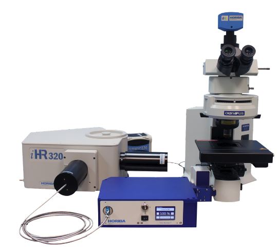
Modular Turnkey Systems Add Spectroscopy to any Microscope

News

HORIBA Scientific, global leader in fluorescence and Raman instrumentation and other spectroscopy solutions, is proud to be introducing its new Standard Microscope Spectroscopy (SMS) systems today at the Photonics West conference, in booths 1950/1951.

With its unique set of accessories, the SMS family of systems enable any standard microscope to be fitted with a spectrometer and a detector, thereby offering the ability to perform techniques such as Raman, steady state and time-resolved Photoluminescence, Reflectance/Transmittance, Electroluminescence, Photocurrent and Dark Field Scattering. The SMS platform brings unprecedented flexibility and modularity to performing spectroscopy on standard microscope systems, all without compromising the imaging functionality of the microscope.

The concept driving these systems is the ability to either leverage an existing standard microscope, or create a fully turnkey system that performs the microscopy function, and adds one or more spectroscopies as a complementary technique. Multitask your microscope™ is the theme behind these Standard Microscope Spectroscopy (SMS) systems.

The Optical Spectroscopy Division specializes in custom configurations with spectrometers, monochromators, microspectroscopy, CCD’s and other instruments for fluorescence spectroscopy and other R&D and QC applications. They design systems that meet customers’ individualized research or application needs. The OSD group specializes in designing the tools required to assist investigations when standardized tools do not meet the needs or where no tools currently exist. The division also sells spectroscopy components for user-built systems.

Purdue, imec, Indiana announce partnership
Resilinc partners with SEMI on supply chain resilience
NIO and NXP collaborate on 4D imaging radar deployment
Panasonic Industry digitally transforms with Blue Yonder
Global semiconductor sales decrease 8.7%
MIT engineers “grow” atomically thin transistors on top of computer chips
Keysight joins TSMC Open Innovation Platform 3DFabric Alliance
Leti Innovation Days to explore microelectronics’ transformational role
Quantum expansion
indie launches 'breakthrough' 120 GHz radar transceiver
Wafer fab equipment - facing uncertain times?
Renesas expands focus on India
Neuralink selects Takano Wafer Particle Measurement System
Micron reveals committee members
Avoiding unscheduled downtime in with Preventive Vacuum Service
NFC chip market size to surpass US$ 7.6 billion
Fujifilm breaks ground on new €30 million European expansion
Fraunhofer IIS/EAS selects Achronix embedded FPGAs
Siemens announces certifications for TSMC’s latest processes
EU Chips Act triggers further €7.4bn investment
ASE recognised for excellence by Texas Instruments
Atomera signs license agreement with STMicroelectronics
Gartner forecasts worldwide semiconductor revenue to decline 11% in 2023
CHIPS for America outlines vision for the National Semiconductor Technology Center
TSMC showcases new technology developments
Alphawave Semi showcases 3nm connectivity solutions
Greene Tweed to open new facility in Korea
Infineon enables next-generation automotive E/E architectures
Global AFM market to reach $861.5 million
Cepton expands proprietary chipset
Semtech adds two industry veterans to board of directors
Specialty gas expansion
×
Search the news archive

To close this popup you can press escape or click the close icon.
Logo
×
Logo
×
Register - Step 1

You may choose to subscribe to the Silicon Semiconductor Magazine, the Silicon Semiconductor Newsletter, or both. You may also request additional information if required, before submitting your application.


Please subscribe me to:


You chose the industry type of "Other"

Please enter the industry that you work in: