Atomic-scale memristive devices: small, smart and scalable

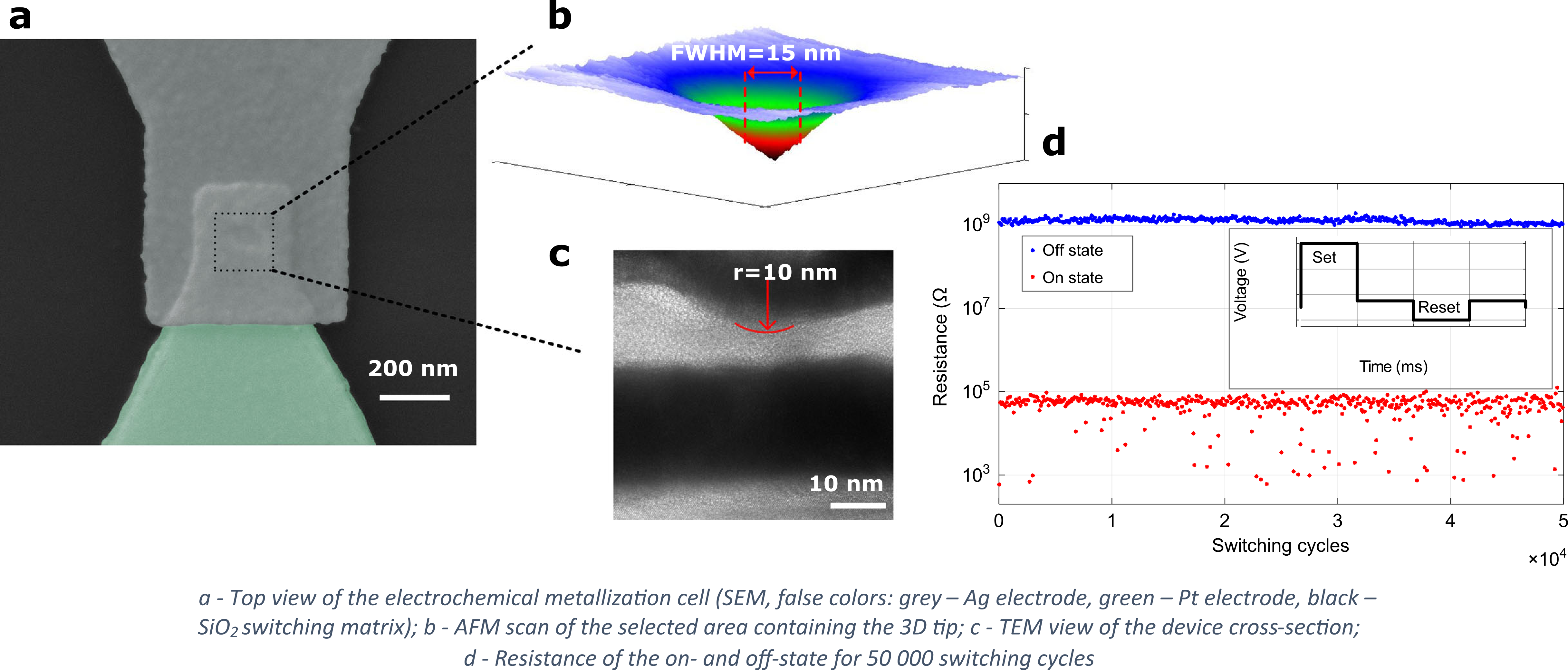
Atomic-scale electrochemical metallization cells enabled by the NanoFrazor were demonstrated by Bojun Cheng and his colleagues from Prof. Leuthold’s group at ETH Zürich. Electrochemical metallization cells (EMC), or conductive bridging random access memory (CBRAM), usually consist of metal-insulator-metal layer stacks, where one metallic player plays a role of an active electrode, and the other – of the inert one. To switch between different states, the cell electrochemically grows or dissolves a tiny metal filament between the electrodes. EMCs reported in Communications Physics feature low switching voltage around 100 mV, operation speed in the nanosecond range, extinction resistance ratio as high as 6 × 10⁵, reliable operations, and the possibility to achieve multi-level behavior.
Such impressive performance at the atomic scale is achieved due to the device geometry: one of the electrodes (Pt) is flat, whereas the other one (Ag) is essentially a 3D tip about 10 nm in radius, creating a highly confined electric field in a few nm-thick SiO2 switching matrix. The tip geometry was defined in the PPA resist using the NanoFrazor and then transferred into the SiO2 by reactive ion etching. During switching, a few-atoms long filament forms between the electrodes, acting as a conductive bridge. In such EMCs, filaments suffer little from Joule heating, as they operates near the ballistic limit and most of the power dissipation occurs in the metallic electrodes and not the filament itself.
Reliable performance together with nm-scale footprint make such EMCs very promising for non-volatile memory applications. With help of thermal scanning probe technology, fabrication of such devices can be significantly scaled up without compromising the dimensions of 3D tip.


