Dual-layer approach advances WLP performance
Improvements across the advanced packaging landscape have already addressed many performance requirements for reducing total thickness variation (TTV) and warpage while lowering costs and improving throughput. A major hurdle remains: extreme temperature survivability. According to Brewer Science experts, winning this advanced packaging 'last frontier’ requires a dual-layer approach.
The drive to create next-generation electronic devices begins with a sound foundation. While the largest IC makers are pushing CMOS scaling to 7 nm and below, other advanced circuit manufacturers are taking a different route to high performance, including the adoption of 2.5D/3D architectures that reduce footprints while increasing speed and functionality.
Manufacturers have succeeded in dramatically reducing TTV and warpage with high throughput and lower costs by utilizing various wafer thinning and materials technologies that support an assortment of packaging platforms. Wafer-level chip-scale packaging (WLCSP) is attractive due to its ability to deliver high performance at low cost. But since it utilizes a ‘substrateless’ package, applications can be limited due to die size. Alternatively, fan-out wafer-level packaging (FOWLP) technology is being widely developed because input/output (I/O) density can be increased by fanning out interconnects to external pad locations, thereby achieving a smaller form factor (and/or smaller footprint) with decreased power consumption.
The next big hurdle for advanced packaging—some say the most challenging—is maintaining state-of-the-art performance, stability and throughput while adding the ability to withstand high-temperature annealing and deposition steps. This is complicated by the industry’s need to thin wafers to a much greater degree than was utilized in older-generation devices. Today’s wafers are often thinned to well below 30 µm. Processing such thin, brittle wafers ultimately requires a carrier system for handling high-value substrates through subsequent downstream processes that include high-temperature anneal and deposition steps.
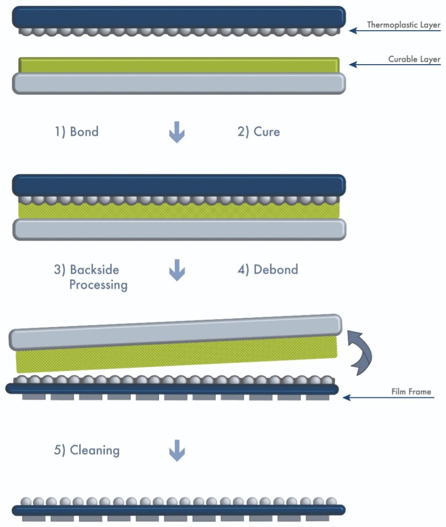
Figure 1: The Brewer Science TBDB process flow in typical WLP/FOWLP applications
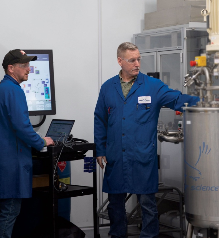
Handling thinned substrates is a major challenge within semiconductor manufacturing. Silicon wafers less than 50 µm thick or those with redistribution layers (RDLs) created using an RDL-first process are delicate and expensive to manufacture. Safe handling necessitates the use of support substrates and processing steps that utilize temporary bonding and debonding (TBDB) materials designed to enable complex packaging infrastructures.Temporary bonding materials created using high-viscosity, low-Tg thermoplastic polymers are commonly used in TBDB processes. When paired with a supportive carrier, these materials offer thermo-mechanical stability and easier handling of the thin device substrate. While the extensive selection of TBDB materials offered by Brewer Science supports many bonding/debonding techniques (mechanical, laser, chemical and so forth) the introduction of higher-temperature steps can cause these materials to behave more like a liquid; as a result, temporarily bonded wafers lose mechanical stability as melt viscosity decreases. This allows some material to soften, weakening bond line stability.
Deformation and delamination of the device wafer can occur at higher temperatures, which leads to downstream processing issues. Brewer Science takes the extra steps needed to provide customers a TBDB system that eliminates common material failure points.
Solutions for any WLP approach
Advanced packaging techniques are designed around either a ‘chip-first’ or ‘chip-last’ process sequence. While chip-first has its advantages, it also uses die that are untested, which can reduce final yield. In chip-first processes, singulated die are placed onto a substrate that has been process coated with temporary bonding material or thermal release tape (TRT) prior to being encapsulated with epoxy mold compound (EMC) in a thermocompression process.
But high-temperature dielectric processing induces stress and leads to warp between the carrier wafer and EMC, which can decrease yield and device performance. Die shift and die stand-off due to substrate warpage and bonding material softening during EMC processing creates RDL misalignment to the embedded die.
In a chip-last process flow, glass carrier wafers are coated with a removable laser release material that creates a foundation for building the RDL. The laser release material needs to possess good thermal, mechanical and chemical stability to survive thinning as well as backside dielectric and deposition processes.
Both chip-first and chip-last process flows require the use of high-temperature and high-vacuum steps to create the RDLs. Today’s FOWLP processes require materials that can survive high temperatures and harsh chemical environments while maintaining mechanical stability.
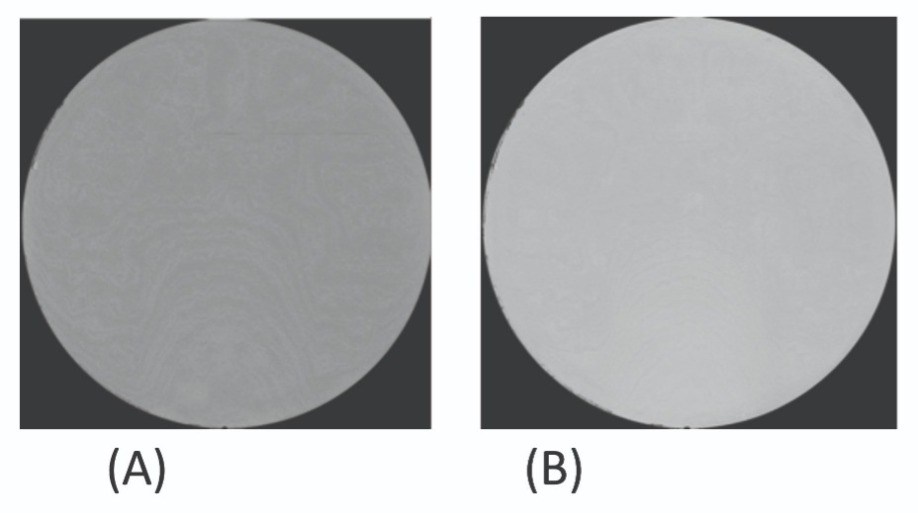
Figure 2: Images from a scanning acoustic microscope shows (A) no heat treatment and (B) after heat treatment
BrewerBOND materials for FOWLPBrewer Science has released two new lines of products to support rigorous advanced packaging requirements. Introduced at SEMICON Taiwan in late 2018, the BrewerBOND® T1100 and C1300 series materials deliver next-generation bonding system performance that enables high throughput as well as high thermal stability. The materials also provide room temperature bonding and debonding for both wafer-level and panel-level processing. These two advanced materials support wide-ranging manufacturing requirements, enabling more uniform post-grind thicknesses of <50 mm while also enabling device structures (and the temporary bond) to survive heat treatment under vacuum. Figure 2 shows a scanning acoustic microscope (SAM) image of a bonded wafer pair after thinning with a 30-minute 400°C heat treatment under vacuum, providing a defect-free bond line without damage to the device.
According to Kim Yess, Brewer Science Technology Director for Wafer-Level Packaging Materials, the dual-layer approach of the BrewerBOND materials series has key advantages compared to materials with less complex or less capable formulations.
“The BrewerBOND T1100 series materials are designed to conformally bond to device structures; the materials have specific rheology attributes for exceptional coating and protection of device structures. The BrewerBOND C1300 series material is a curable thermoset layer that remains malleable until final cure,” she said.
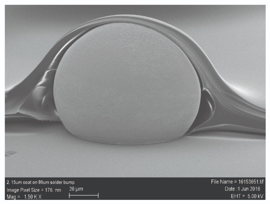
Figure 3: The BrewerBOND T1100 material delivers highly conformal coating and adhesion preperties
Yess explained that the dual layer system is comprised of a low-Tg thermoset material (BrewerBOND C1300) applied to a carrier. This assembly is then bonded to the device wafer that has been processed with the corresponding high-Tg bonding material (BrewerBOND T1100) that coats device structures. After bonding and processing at room temperature, the pair can then either be UV exposed or hotplate baked to cure the thermoset material. When processed below 350°C, the BrewerBOND T1100 series material remains solvent-soluble and has little to no melt flow up to 300°C. When coated, this material is highly conformal and even when applied thinly it can cover severe topography. Figure 3 shows a scanning electron microscope (SEM) cross-section of a 2.15 µm film of BrewerBOND T1100 series material processed over 80 µm solder bumps.Yess explained the exceptional performance achieved by their dual-layer approach was developed by Brewer Science to optimize the coatings’ most essential qualities while making various application steps fit into typical process flows at high throughput levels. (See Table 1 for key materials properties.)
“The BrewerBOND T1100 and C1300 materials need each other to perform to their optimal potential. The BrewerBOND T1100 material is thinner, relatively speaking, and more conformal, which manufacturers need to address ever-shrinking device geometries. It also enables easier downstream cleaning of the device. BrewerBOND C1300 material creates better stability at higher temperature processes, which reduces warpage and helps ensure post-processing functionality of the devices being packaged,” she said, noting that using the BrewerBOND C1300 material by itself would only do part of the job.
“Manufacturers are building up device layers at nanometer scale much the way we might build a much larger structure: one layer or ‘floor’ at a time. It’s a bit like using concrete when building a home. If you put concrete directly on some structures going into the home it would be hard to clean and would likely damage the most sensitive structures. But by using the right coatings, semiconductor manufacturers can achieve the stability and temperature resistance they need at nano scale while still retaining the ability to remove coatings when needed simply by using industry-standard cleaning processes and chemicals,” she explained.
BrewerBUILD materials advance RDL-first applications
Designed specifically for RDL-first applications, BrewerBUILDTM materials are single-layer, high-absorbing materials for buildup and assembly; they are designed for use in laser ablation processes. These materials have increased absorbance at wavelengths between 308 and 355 nm and offer increased protection to the device wafer during laser ablation. This new generation of materials also offers strong solvent resistance and high adhesion to many materials and they respond very efficiently to solvent cleaning after ablation.
“The BrewerBUILD family of materials addresses pain points experienced by customers associated with RDL-first applications. This technology is designed to optimize dielectric materials for RDL layers, resolving features down to 2 mm, offering higher I/O density for advanced packaging architectures. The material is designed to address challenges that include bridging the gap in the available I/Os at both die and board levels, high performance requirements, integration and form factor demands from end users, as well as design and process complexity of fan-out packages,” Yess stated.
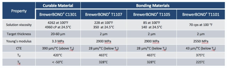
Table 1: Properties of BrewerBOND advanced materials
“In order to maximize KGD and minimize yield loss, BrewerBUILD materials can be coated at the wafer and panel levels, and provide in-process thermal and mechanical stability,” she explained. “These benefits extend to polyimide (PI) cure and molding. The materials deliver strong adhesion to metals such asTi and Cu as well as polymers including PI; the materials provide excellent chemical resistance, too.”
“BrewerBUILD materials enable excellent laser debonding, featuring high light absorption to protect device wafers from laser damage. There is also low to no carbon residue after laser debonding, which enables easier cleaning and better levels of carrier reclamation,” she stated.
Summary
Brewer Science brings high level materials expertise to advanced packaging that is paving the way for innovation through the use of new temporary bonding/debonding materials that uniquely support FOWLP technology requirements. When combined into a system, BrewerBOND dual layer materials impart improved mechanical stability that reduces the hazards of handling thinned, bonded wafers that need to undergo high-vacuum or high-temperature processing. The materials’ conformal nature, room-temperature bonding/debonding characteristics and chemical resistance provide added value and improved performance while reducing cost of ownership.
For RDL-first packaging processes, BrewerBUILD materials support build-up and assembly, offering
a better alternative to thermal release tapes. These new materials facilitate low-energy laser debond processes that deliver improved protection for the device wafer with low carbon residues. As packaging techniques continue to evolve, geometries shrink even further and 3D device structures capture increasingly larger shares of overall semiconductor production, count on Brewer Science to develop and deliver advances in bonding and debonding materials to facilitate manufacturers’ requirements. Brewer Science supports next-generation FOWLP technology and is formulating new materials to support emerging device packaging innovations
now under development.