
Comparing PTFE and PFA fluoropolymers as wetted parts in advanced semiconductor manufacturing
Industry experts examining two types of fluoropolymers used to construct semiconductor process chemical containment vessels have concluded that the type of polymer utilized can affect the potential for particle contamination, a concern that grows more critical at each new device node.
Jorge Ramirez, President & CEO, Heateflex Corporation; and Stephane Domy, Global Marketing Manager, High Purity Systems, Saint-Gobain
Semiconductor manufacturing incorporates a number of wet process steps in the construction of a microchip. Liquids such as deionized water and various solvents are often used in-between the various manufacturing steps to clean the surface of the wafer and to remove residual photoresist, for example. Other more aggressive acids may also be used in a wet etch process step to help form the lines and vias of the semiconductor device itself.
In these wet process steps, the cleaning or etching fluid being used is often heated to improve its efficiency. Various fluid heaters have been developed for use in semiconductor manufacturing, and these heaters are often constructed using fluoropolymers for the wetted parts (i.e., the portion of the heater actually coming into contact with the fluid to be heated). Two particular types of fluoropolymers are typically used in these applications: Polytetrafluorethylene (PTFE) and Perfluoroalkoxy (PFA). PTFE is found extensively in wetted parts in pumps and valves, and in other applications where the number of parts required are too small to justify the tooling costs required in manufacturing PFA wetted parts. This article will examine the appropriateness of each material for use on the wetted surfaces of semiconductor fluid heaters, and in particular in manufacturing the next generation of microchips.
Advanced semiconductor devices are now being manufactured at device geometries of 10 nm, and several of the largest chipmakers have announced plans to start ramping manufacturing for the 7 nm technology node. At these dimensions, the chip’s circuitry is incredibly dense, and particulate contamination, which can lead to chip failure, is a major concern. The manufacturing equipment used to build these leading-edge chips, then, must be designed to ensure process purity. And while both PTFE and PFA are high purity materials, have exceptional resistance to corrosive chemicals and harsh environments, and are excellent barrier materials due to their low diffusion coefficient, one of these two materials appears to be less susceptible to contamination, and hence is more suitable for use in wetted parts in sub-10 nm manufacturing.
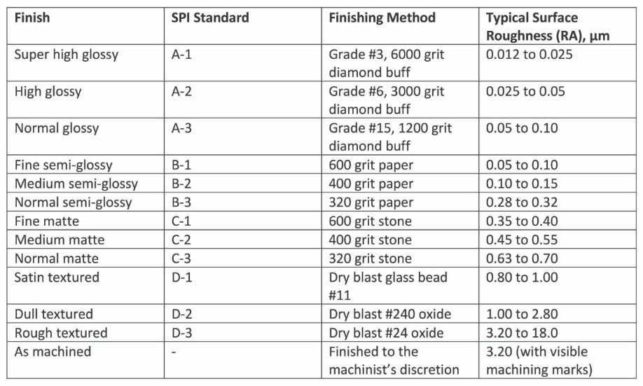
Table 1. SPI Mold Finishes
In terms of their properties, PTFE and PFA parts are similar, but there are differences in how they are manufactured. It should be noted at the outset that the manufacturing process used to create PFA parts is more costly than that used to create parts made of PTFE. The manufacturing process sequence, though, is key to each material’s suitability for use in manufacturing advanced semiconductor chips, as will be shown in the following paragraphs.
First and foremost, due to its high melt viscosity the molecular structure of PTFE will not allow the material to flow when heated. Because of this, PTFE parts are typically made using a multi-step process. First, the powdered PTFE resin is poured into a mold, and then compressed under high pressure. It should be noted here that these initial process steps in and of themselves carry a medium-level risk of introducing contaminants into the PTFE raw material. Next, the block of PTFE is sintered, followed by an adaptive cooling step based on the shape and size of the block. Finally, the PTFE material block is machined to the appropriate shape, another process step which runs the risk of contamination. If the PTFE part block is dry-machined, there is a relatively low-level risk of introducing contaminants. The risk of contamination grows higher, though, if the PTFE block is wet-machined.
In contrast, the molecular structure of PFA does allow it to be melt processed, and so PFA parts may be made by traditional, one-step processes such as injection molding. When injected, PFA produces a skin at the interface surface of the part that creates a surface roughness that is barely measurable. Therefore, PFA parts may be manufactured without requiring any post-processing machining. This machining step (or lack thereof) does affect the surface finish of the polymer which will be in contact with the semiconductor process chemicals under manufacturing. And as will be shown in the subsequent paragraphs, the surface finish of the wetted parts is key to their ability to repel (or absorb) potential contaminants when in use. The Society of the Plastics Industry (SPI) has identified plastic surface finishes and their corresponding Roughness Average (RA). The SPI findings are show in Table 1.
As shown in the table, machined plastic parts such as those made with PTFE typically have a 3.20 RA value. In contrast, most mold-injected parts such as those made with PFA meet the B-1 SPI standard or higher, with a typical surface roughness of 0.05 to 0.10 µm (B-1). The PFA parts, then, have a 98.4% smoother finish than their PTFE equivalents.
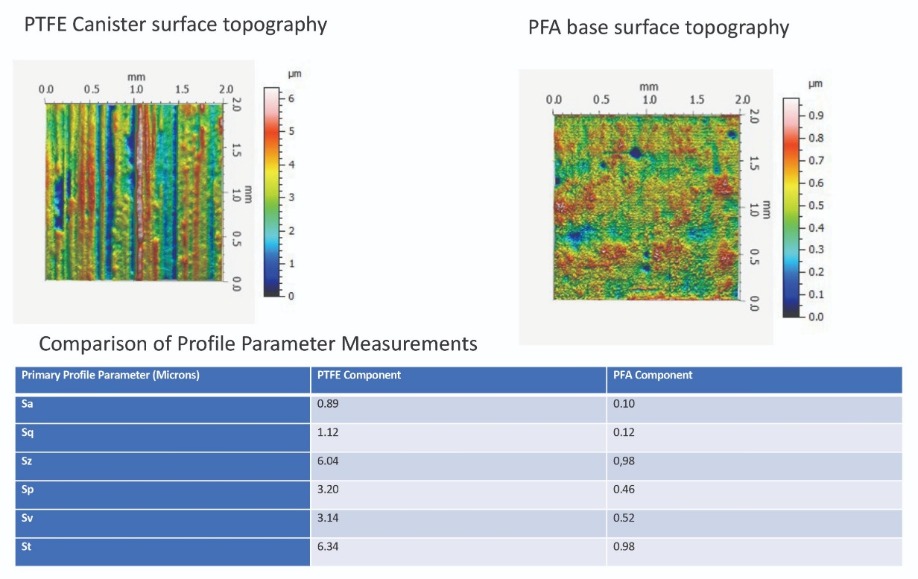
Figure 1. Surface Roughness Comparison
With shrinking device geometries, the surface roughness of a material used as a wetted surface in semiconductor manufacturing becomes more critical as demands for higher purity increase, since the surface roughness is directly linked to particle generation.Due to all of these considerations, Heateflex Corporation, a manufacturer of fluid heaters used in semiconductor manufacturing, and Saint-Gobain’s High Purity Systems business unit, a global supplier of fluoropolymer-based fluid management solutions for the semiconductor industry, decided to examine the surface roughness of various PTFE and PFA components.
First, Saint-Gobain studied the polymer profiles of two different fluoropolymer components, as shown in Figure 1.
These components were examined with a Nanovea 3D Surface Profilometer using a white light chromatic aberration technique. Areas of each component were scanned on the surface at pre-selected areas, with each scan measuring 2.0 mm x 2.0 mm. 3D primary profiles were then calculated for each area scanned, and 3D images of the height data were captured.
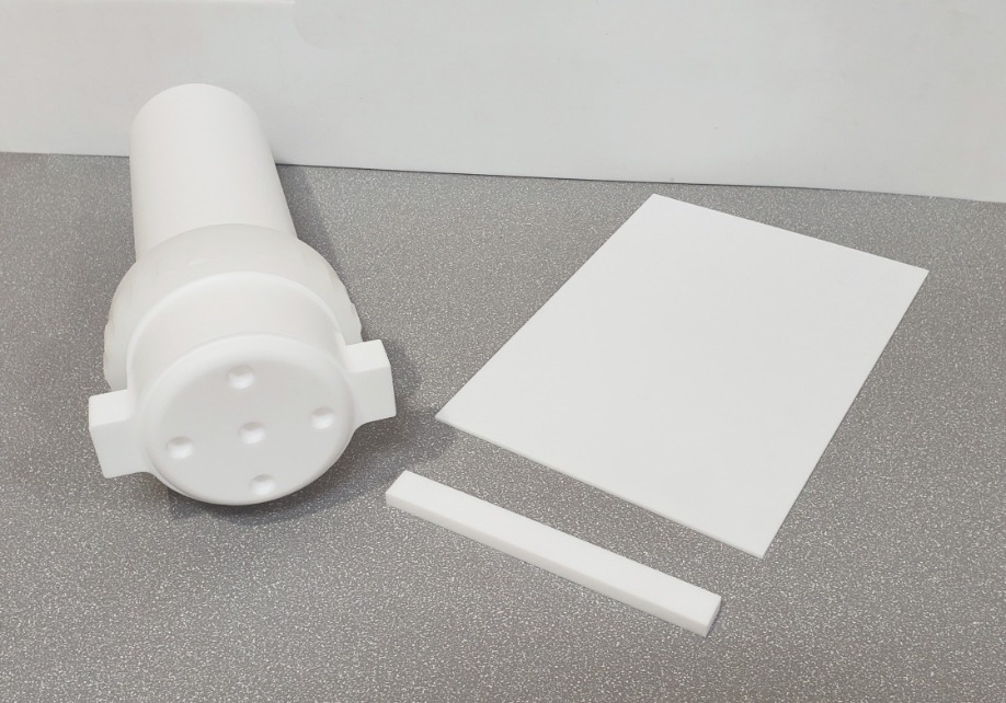
Figure 2. PTFE housing, compression-molded bar, and compression-molded sheet
Amplitude parameters are a class of surface finish parameters that characterize the distribution of heights. Table 2, below, presents the following parameters that are normalized in the ISO 4287 standard for surface textures. Some of these parameters are listed in the EUR 15178 EN report. The reference plane for the calculation of these parameters is the mean plane of the measured surface.As Figure 1 demonstrates, the maximum heights of the summits (Sp) of the sample PTFE part were 6.96 times higher than those in the PFA part, and the maximum depth of the valleys (Sv) in the PTFE part were 6.04 times deeper than those in the PFA part. Overall, then, the PFA component offers a surface finish that is at least 6 times smoother than the PTFE component on all profile parameters measured.
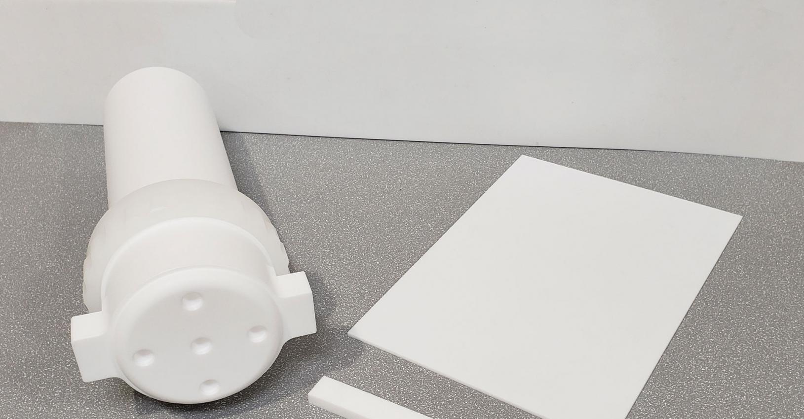
Then, to supplement the Saint-Gobain profile parameter measurements of these two materials, Heateflex conducted a simple experiment to test their resistance to particle contamination. Several parts manufactured from PTFE were assembled: a housing, a compression-molded bar, and a compression-molded sheet (see Figure 2).
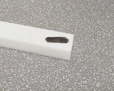
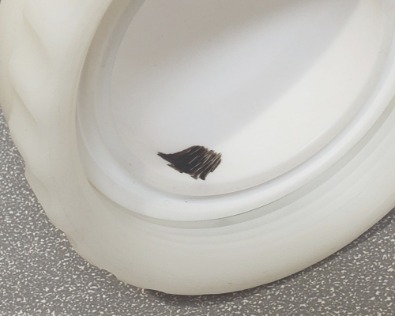
Figure 3. PTFE bar and housing marked with dry erase marker
These parts were then marked with a dry erase marker, as shown in Figure 3. The dry erase marker was chosen due to its ready availability. It also allowed the experiment to be easily duplicated, and provided non-permanent pigmentation.Note that the PTFE materials in the photos appear to have a hydrophilic behavior. The liquid from the marker creates good surface wetting.
After 5 seconds, the marks were wiped away using a dry paper towel. After the liquid is removed from
the surface, though, pigment from the marker appears to remain embedded in the material, as shown in Figure 4.
This same experiment was then repeated using an injection-molded housing and an extruded pipe made of PFA materials (see Figure 5). The same wetting process that was used on the PTFE parts (i.e., marking with a dry erase marker) was repeated on these PFA parts.
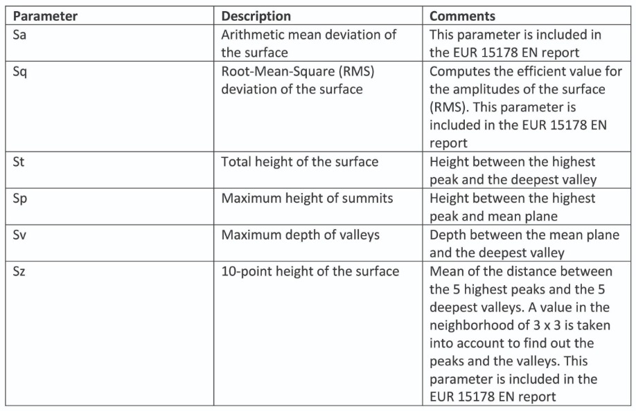
Table 2. Summary of surface measurement parameters
As shown in Figure 6, the PFA materials rejected the liquid from the dry erase marker. The smoother finish and the material characteristics make the PFA appear to have a hydrophobic behavior: the liquid from the marker puddles together and does not create good wetting. After the mark is wiped away, the material remains in its clean state. Pigment does not embed in the PFA material, as it did in the PTFE parts.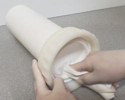
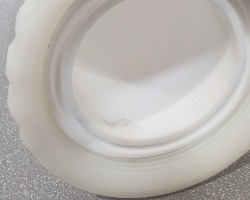
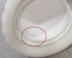
Figure 4. PTFE compression-molded/machined housing after wiping with a dry paper towel. Pigments from the liquid marker remain embedded in the material
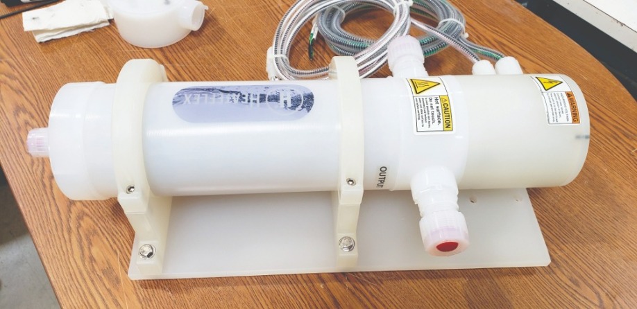
Figure 5. PFA housing (injection molded) with extruded pipe
ConclusionIn conclusion, then, while both PTFE and PFA fluoropolymer materials have been adopted for use in semiconductor manufacturing, it appears that the PFA materials are better suited for wet process fluid heating in manufacturing the next-generation of sub-10 nm microchips. First, the one-step injection-molded PFA manufacturing process is inherently less likely to introduce contaminants into the component being formed than is the PTFE manufacturing process sequence. Secondly, due to the smoother surface finish, the PFA material is a superior candidate for preventing particle shedding. Finally, PFA raw materials are now being monitored to a SEMI standard to ensure cleanliness. There is no comparable standard at the present time to monitor the cleanliness of PTFE powder, and none is anticipated.
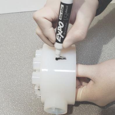
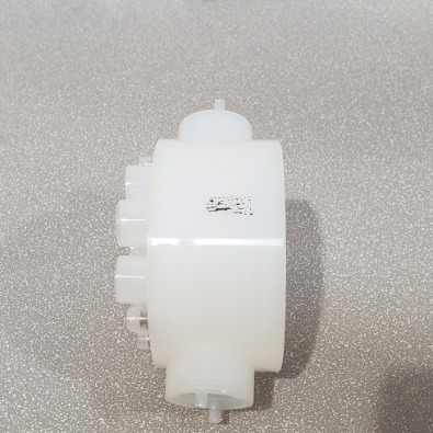
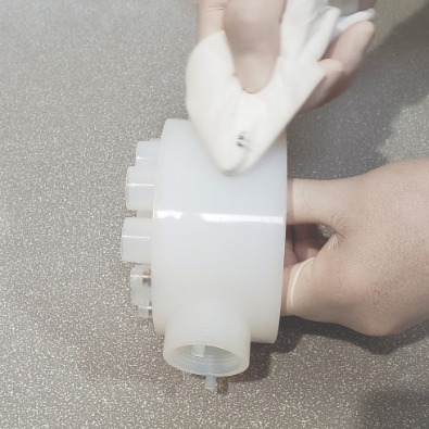
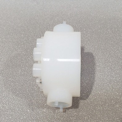
Figure 6. PFA housing marked with the dry eraser, and then wiped clean. No pigments remain on the PFA material


