Semi-automated multi-station systems boost wafer processing speed, quality & repeatability

Logitech describes key advantages of its new LP70 multi-station automated lapping and polishing system that can dramatically increase overall wafer productivity by 40 percent for almost all substrate materials.
The lapping and polishing of wafers used to manufacture semiconductors and optical devices is a time consuming task that can risk damage to expensive custom wafers worth in excess of (USD) $5,000 each if things do not go to plan. Logitech has substantially automated the process, speeding productivity and increasing repeatability by approximately 40 percent compared to non-automated techniques.
In wafer end fabrication, lapping and polishing processes have become more predictable, but there is often the need for a significant level of user expertise, guesswork and development time in order to optimise surface finish and repeatability. This can hamper the development of new technologies, especially as a process that is optimised at the pilot stage will often need to be revisited when transitioned to full production.
The path to better process control lies within Preston’s Law which provides a framework for predicting the amount of material that will be removed in a given time by lapping and polishing processes. By controlling variables using automated precision lapping and polishing systems with high levels of user control, operator variability can be minimised while process accuracy and greater repeatability can be achieved.
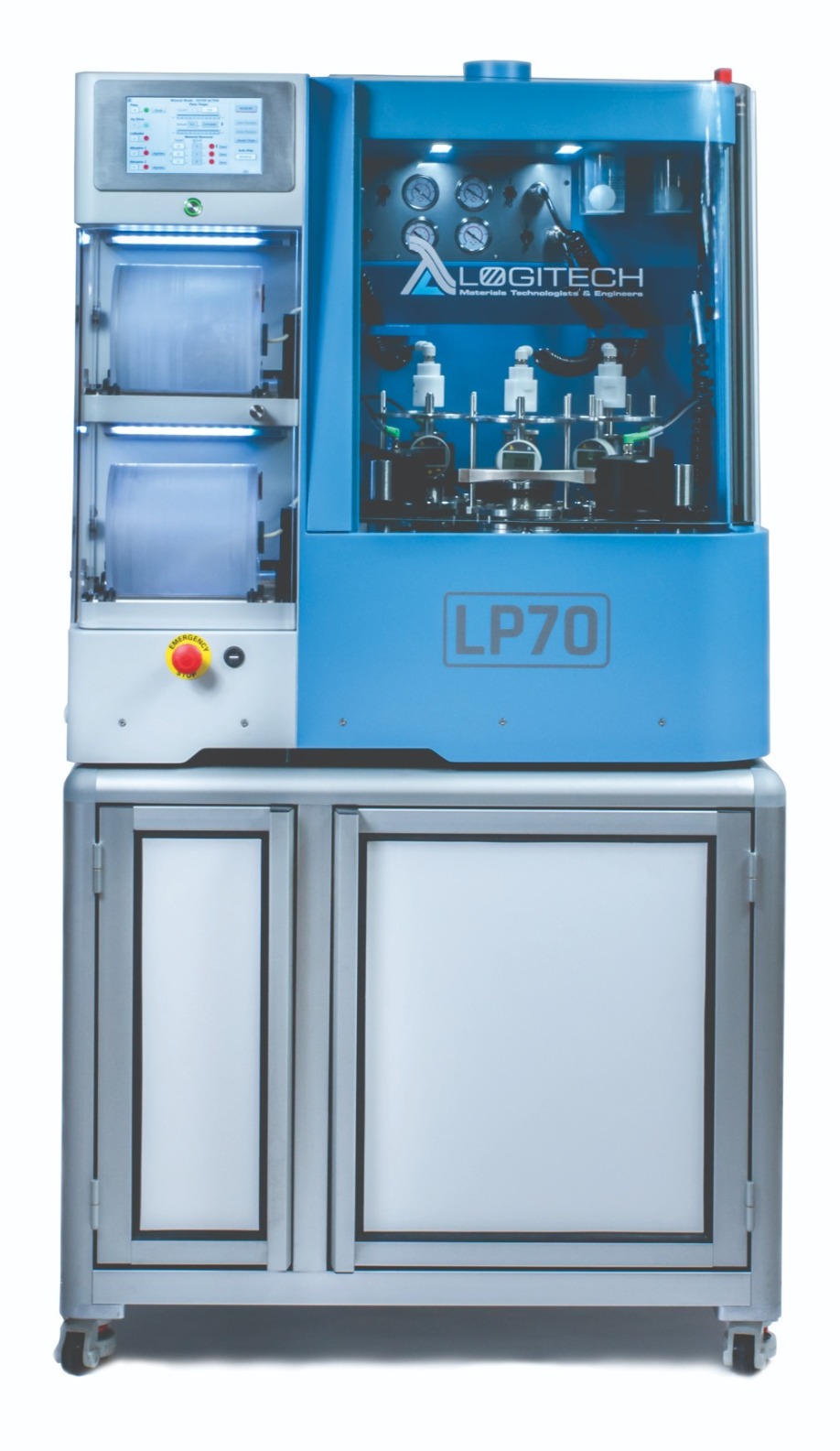
The Preston’s Law equation states that the material removal rate (MRR) is proportional to the product of the processing pressure/load/down-force and plate velocity. In the chemical mechanical polishing (CMP) process, polishing rates and overall accuracy are affected not only by the flow of the slurry and the characteristics of the polishing plate, but also by the mechanical action between the wafer and the plate, chemical reactions arising from slurry component molecules, and the interactions between these variables. Preston’s Law can be used to accurately predict the amount of material removed from a sample and confirm stability in the process. High degrees of process stability are possible by using a stable/accurate/repeatable processing platform such as the Logitech LP70 Multi-station Precision Lapping & Polishing System, which can process up to four 100mm or two 150mm wafers simultaneously.
Meeting demanding wafer requirements using manual lapping and polishing tools is hard to achieve with silicon, III-V or other very hard semiconductor wafer materials because of the high level of operator skill needed to manually stage and control such operations. Setup is a time consuming process that is not conducive to the high productivity that is demanded by semiconductor research and production facilities. Cost reduction in device production is driven by volume and yield. Automated systems designed to eliminate manual steps will ultimately increase productivity in wafer fabrication processes. The use of multiple work stations for simultaneous wafer processing will allow operators to achieve high throughput levels to keep up with the demand of their application.
Logitech’s Robin Armour, Process Development Engineer, frequently works with customers in the field who appreciate the precision of an automated systematic approach to wafer lapping and polishing. Robin has also been instrumental in the development of the LP70’s intelligent functionality to ensure it meets demanding customer requirements.
He notes that since the successful launch of the Logitech PM6 Precision Lapping & Polishing system, there has been increasing demand from both new and repeat customers based on the success of the PM6’s automated features.
“One requirement we see real demand for is increased levels of throughput on a single system whilst maintaining automated processes. The LP70 system has been developed from the same automated features as the PM6 with the increased throughput levels achievable to operators utilising four workstations on a single system rather than using multiple units – allowing for further cost reductions,” he remarked.

Silicon lapping & polishing
Every semiconductor wafer undergoes several common processing stages during manufacture including slicing the wafer from its crystal ingot, preparing the surface prior to fabrication and subsequent thinning of the wafer through lapping and polishing techniques.
After slicing, wafers made of silicon or III-Vs materials are lapped to remove surface scratches and flaws that occur during cutting processes. Typically performed by the wafer manufacturer, lapping removes saw marks and surface defects from the wafer and also helps relieve any internal mechanical stress that accumulated during the slicing process.
Lapping typically involves counter-rotating plates using an aluminium oxide abrasive with defined grain size distribution. During lapping, wafer flatness is improved while micro-roughness is also reduced. An edge grinding procedure may also take place. When edge grinding is needed manufacturers may also follow this step with polishing the wafer edge since doing this can greatly reduce the probability of wafer breakage further down the process line. Chemical mechanical polishing is the final material removal step utilized in manufacturing wafers. This process allows the attainment of super-flat, mirror-like surfaces with a remaining roughness on an atomic scale. Polishing the wafer can be seen as the most crucial step in the wafer manufacturing process since the polished wafer face is used as the base for device fabrication; it must be as damage free as possible. Typically, optimized CMP is achieved using a rotary or orbital motion of a chemical slurry injected in precise quantities and flow rates between the polishing plate and the wafer itself.

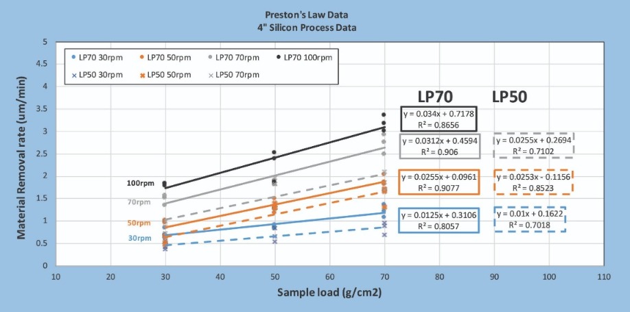
Chart 1: The chart illustrates performance advantages of Logitech’s LP70 compared to a predecessor system with fewer automated capabilities, the LP50. Utilising Preston’s Law in combination with other system enhancements, the LP70 can deliver approximately 40 percent total process time savings.
There are many reasons why manufacturers need stability and repeatability when it comes to wafer sample preparation. For instance, stringent quality requirements dictate that parameters such as total thickness variation (TTV), surface roughness and plate flatness must be carefully monitored. In all cases, a fundamental understanding of the process is required to ensure a quality outcome. Different types of wafer materials, slurries and polishing pads, along with polishing rate, pressure and uniformity can all impact the resulting surface. It is also important not to overburden the surface with too much slurry as this has the potential to impair detection of when the polishing process is complete. To put this in simple terms, it is vital to accurately predict the amount of material removed from a sample in a given time. Here, Preston’s Law is fundamental to successful lapping and polishing. Indeed, it is possible to analyse the Prestonian behaviour of material removal rate (MRR) to confirm that all-important process stability has been achieved.The LP70 has the ability to chart the removal rate data from the process jig and auto-plate flatness monitor in real-time utilsing the time weighted average (TWA) functionality. With this there is a need to accurately control the process by either stopping or programming an event action when the removal target has been reached, for instance, based on interaction of the process variables (plate type, speed, slurry flow rate, etc.) There is then the need to use data averaging to ‘smooth’ the process noise for increased accuracy on the target removal, using the central limit theorem. The amount of averaging is listed as a user control input field in the software, so the operator can optimise their process according to various needs. Removal rate data can be plotted real-time on the LP70’s graphical user interface (GUI); data can also be exported for further analysis via USB. This functionality allows operators to achieve increased levels of accuracy within their process that is easily repeatable.
Silicon lapping & polishing trials with the LP70
Lapping and polishing trials using a typical silicon substrate deployed in semiconductor applications such as manufacturing integrated circuits, solar cells and waveguide devices can be extremely revealing. In trials with the LP70, a series of steps was used, each with a different slurry solution, in sequence designed to replicate the steps a customer would typically undertake if they were lapping and polishing a production wafer.
Firstly, a coarse lapping process is utilized to remove material within 50 µm of the end point target. Previous experiments have shown that slurries containing AI2O3 particles measuring 20 µm provide the optimum balance between material removal speed and maintaining the integrity of the underlying silicon wafer. In a second stage, a medium/fine lapping process is conducted, during which a finer, less abrasive 9 µm AI2O3 slurry is used to remove materials to within 10 µm of the end point target. The final stage involves removing the last micrometres of material; the removal of any damage caused to the wafer during the lapping process is also undertaken using 32nm colloidal silica, such as the Logitech SF1 polishing slurry. After undergoing all three stages a typical surface roughness of Ra<1nm is achievable.
Tests with the LP70 to determine average silicon lapping at 50 rpm and 70 rpm showed an average 25 percent increase of material removal rates (MRR) in comparison to the LP70’s predecessor system, the LP50, that has fewer automated capabilities. LP70 features that allow for this increase in MRR are mainly: increased plate diameter; metered abrasive slurry distribution to each jig station and the driven roller arm. The LP70 also enables a 50 percent improvement on sample to sample (per workstation) end point thickness variation. Substantial time savings and greater accuracy were also achieved with the LP70’s automated set up and control platform. Collectively, all automation improvements delivered a total process time savings of approximately 40 percent, company research indicates.
Differentiating features found in automated systems such as the Logitech LP70 or PM6 Precision Lapping & Polishing Systems are key to achieving such impressive results. Intelligent controls on both systems have positive impacts on processing that not only benefit by creating a flatter, more defect-free wafer, but also in terms of substantial process time reductions. These technologies can help semiconductor optical device manufacturers to precisely optimise their sample preparation processes.
Conclusion
A high degree of geometric precision, flatness and parallelism can be achieved by taking advantage of automatic wafer thickness control. Software-driven set-up within automated systems permits faster processing times (in tandem with plate speeds of up to 100 rpm) and more reliable results. There is also extensive parameter control for the processing of complex and fragile wafers; metered abrasive feed supplies for optimal processing and reduced wastage of consumables are other substantial cost saving factors. Automated systems like the Logitech LP70 or PM6 also provide for the export of critical data that can be used as an information base for future process refinement and documenting productivity improvements over time.
Semiconductor and optical device manufacturers demand greater process control and real-time data in their quest for improved productivity and reliable, repeatable quality. By utilizing an automated approach in sample preparation such as the Logitech LP70 or PM6, researchers and manufacturers alike can achieve faster throughput, more precisely prepared and polished wafers, all with dependable repeatability that also frees their most highly skilled engineers and technicians to focus on other critical endeavours.
For further information on the capability of Logitech precision systems contact:
enquiries@logitech.uk.com or visit www.logitech.uk.com


