
When x-ray and ultrasound join forces

A pulse of ultrasound traveling through a solid is attenuated as it goes and is reflected and/or transmitted by material interfaces. An x-ray beam is also attenuated but ignores material interfaces. An ultrasonic pulse must be inserted at 90° to the surface, but x-ray can be inserted at almost any angle. The usefulness of these and other differences is described.
By Tom Adams, consultant, Nordson SONOSCAN
A pulse of ultrasound is speeding through a layer of copper at a speed around 4700 meters per second. As it moves, the pulse is mildly attenuated - meaning that it is gradually losing energy (amplitude). Suddenly it runs smack into a layer of cured epoxy. One portion of the pulse sails right across the interface between the two solids and keeps going into the epoxy. The other portion is reflected back, at the same speed with which it arrived, to the transducer that launched the pulse.
An x-ray beam travels through the same copper layer. Like the pulse of ultrasound, it is somewhat attenuated by the copper through which it is moving. When it runs into the wall of cured epoxy, the x-ray beam keeps right on moving; none of it is reflected. What does change is the rate of attenuation, because the beam is now traveling through a different material.
When both an x-ray system and an acoustic micro imaging tool are used on the same sample, examining both images can give information that can shed light on quality control or failure analysis questions. Neither energy form causes any physical damage to the part, and it is hard to think of a physical anomaly that can hide from both.
Because it is part of the electromagnetic spectrum, an x-ray beam’s velocity through a material is so high it requires no attention. When imaging a sample, the size of the beam fired from the x-ray tube expands as it moves. The x-y area of the image (magnification) is adjusted by changing the distance to the target.
The speed of ultrasound through a solid is many orders of magnitude less than the speed of an x-ray beam. A 100 MHz pulse, for example, moves through mold compound at about 3,000 meters per second. And ultrasound is launched not as a continuous beam, but as a pulse whose return echo represents an interface area measured in microns. The echo will become one pixel in the visible acoustic image. The transducer launches thousands of pulses per second as it scans, and, where there is an interface in the line of fire, collects thousands of echoes per second.
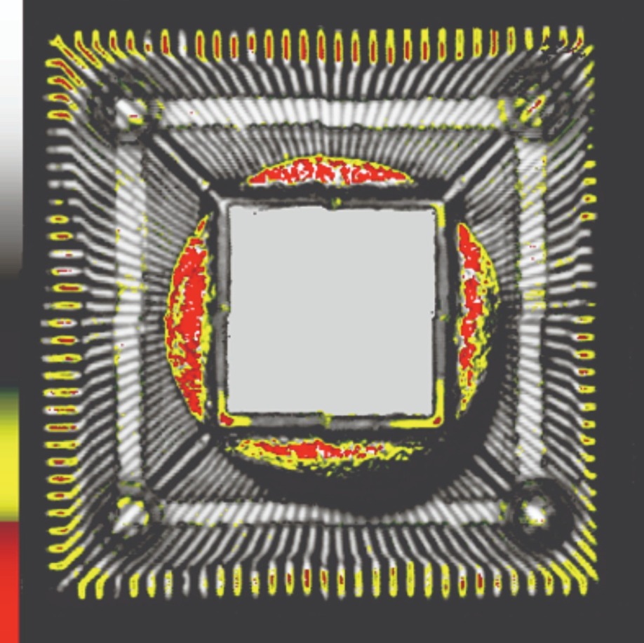
Figure 1: Air gaps in this PEM are red and yellow because they reflect nearly all of the ultrasound. Black regions reflect none.
Figure 1 is the acoustic image of a plastic encapsulated microcircuit (PEM) made by a Nordson SONOSCAN C-SAM® acoustic micro imaging tool. The image was made by accepting for imaging echoes whose arrival times indicated that they originated in a vertical gate ranging from a short distance above the die face to the die attach level. Echoes originating above or below this gate were not accepted. The wires leading from the die to the lead fingers are within the gate, but they are very thin and have a circular cross section that scatters ultrasound. The result is that they reflect too little ultrasound at this frequency to be imaged.Where no echoes were received (between the lead fingers, for example) the pixels are black. The color map along the left side of the image indicates that the echoes reflecting nearly all of the launched pulse are red. The circular red-yellow feature surrounding the die is a crack through the mold compound surrounding the die. The distal ends of most of the lead fingers are also red and yellow.
To the southeast of the circular crack is a curved black area that looks like an optical shadow - but this is an acoustic image. What happened is this: as the crack traveled upward, its path became more vertical. Where it is somewhat level, the crack reflects nearly all of the arriving pulse, and the crack is red. Where the crack becomes more vertical, the crack is yellow (the next color up on the color map at left). Where the path became even steeper, all of the pulse was deflected (echoed) at an angle and no echo was sent upward to the transducer, so the pixels in this area are black (no signal received).

Figure 2: Because x-ray is hardly attenuated by air and not reflected by interfaces, the crack does not appear in this image of the same part.
An x-ray image of the same device was then made by a Nordson DAGE Quadra™ 7 tool and is shown in Figure 2. Ultrasound is reflected by material interfaces, but an x-ray beam sails right through interfaces. The large circular crack in Figure 1 has the solid-to-air interface that reflects virtually all of an ultrasonic pulse, but the crack itself, although lethal, is very thin. The crack cannot be discerned in Figure 2 because it is too thin to appreciably change the attenuation of the beam and thus the brightness of the image in this region.The wires in the PEM shown in Figure 1 were then imaged separately by the Quadra 7 in a region where the wires are bonded to pads on the lead frame (Figure 3). What has happened is clear: the stresses set up by the expanding popcorn crack stretched the wires until they broke and became disconnected from the pads they had been bonded to. The resolution is high enough that details of the break can be seen, along with the wire’s former connection location on the pad.
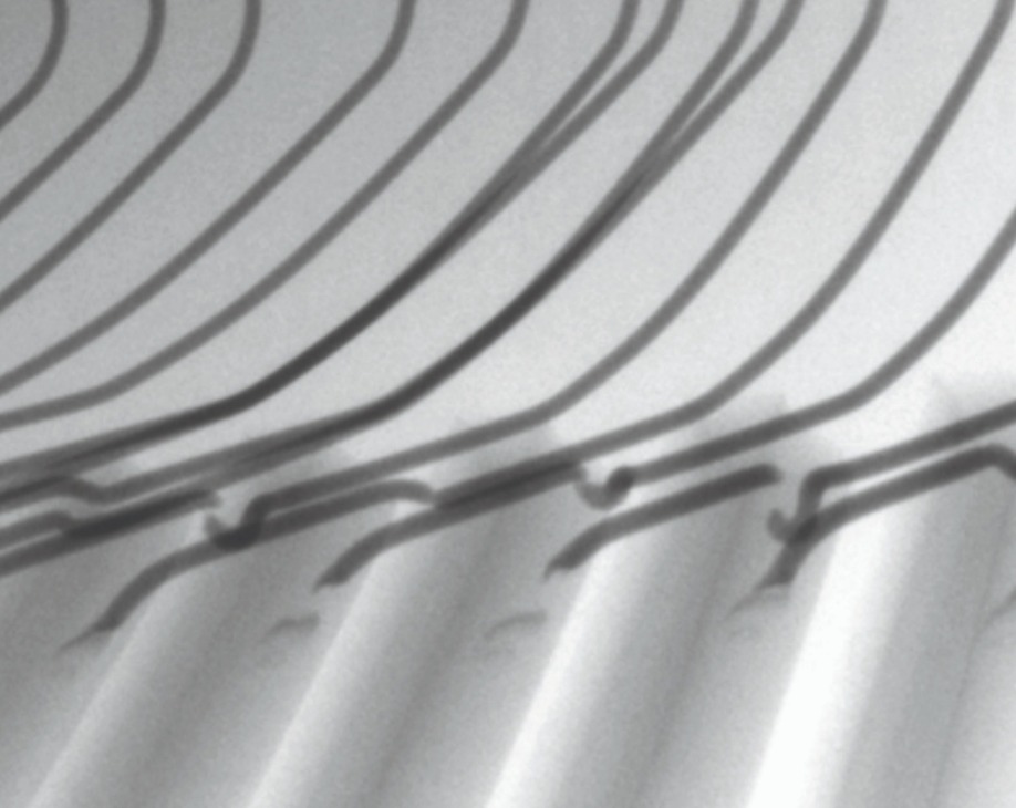
Figure 3: An x-ray closeup of part of the device shows broken wires.
In Figure 1, the resolution in the acoustic image is not sufficient to make the wires visible. At higher ultrasonic frequencies, if a pulse can penetrate the molding compound, wires are sometimes visible, but not in great detail.Figure 4 is the x-ray image of a different device having a die that is eutectically bonded to a ceramic substrate. The lid has been removed to expose the bare die. There is no mold compound. The depth of interest was the die attach, where there may be voids in the eutectic that are efficient blockers of heat radiating from the die.
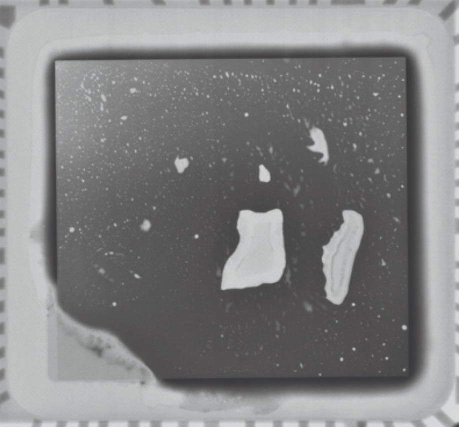
Figure 4: X-ray image of a device having a ceramic substrate and eutectic die attach.
What this x-ray image reveals is that there are hundreds of voids of different sizes where material is missing, all likely formed when the die was put in place and bonded to the substrate. Some of the voids are extremely tiny. They are visible here because the absence of eutectic material results in reduced attenuation of the x-ray beam.At the lower left corner is a very large area where there is no eutectic material, although there are traces of die attach material along the upper right margin of the area. In general, voids in eutectic bonds can form in one of two ways: either the eutectic material melts and flows away, or the pressure applied is not sufficient to make a bond. If the eutectic material is present but did not form a bond, then x-ray will not detect this condition. This large void was probably formed by the melting and subsequent migration of the eutectic material.
The same device is imaged acoustically in Figure 5. Far more voids - and especially tiny voids - are visible here than in the x-ray image. Many voids appear white because they are large enough - even if their overall shape is somewhat spherical - to reflect enough of the pulse to create a visible group of white pixels. Voids smaller than these simply scatter nearly all of the arriving pulse and are black in this acoustic image. Both of the largest voids, which in the x-ray image displayed some internal structure, show no structure here because essentially all of the pulse is reflected by the solid-to-air interface and none enters the void itself.
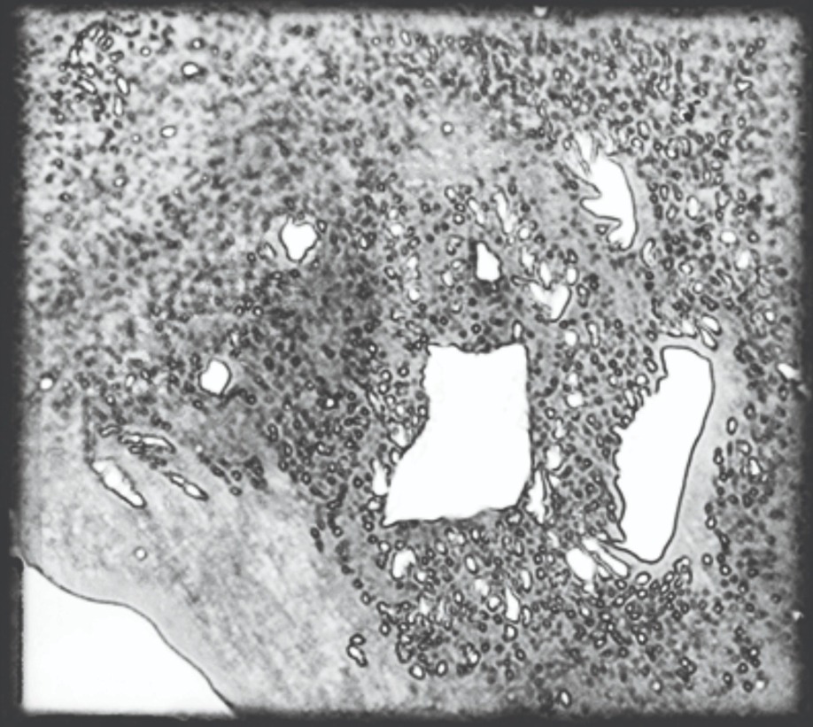
Figure 5: Acoustic image of the same device
A small area near the center of Figure 5 is shown magnified in Figure 6, where it can be seen that even some of the smallest voids have brightly reflecting centers.
Other differing capabilities make it useful to use both x-ray and ultrasound to interrogate a sample. Both are attenuated by solid materials they pass through, but not to the same degree. Ultrasound is rapidly attenuated by materials that are easily deformed, such as polymers, but is far less rapidly attenuated by a material such as ceramic. X-ray is more rapidly attenuated by materials of high density. The metal substrate of an IGBT module, for example, easily transmits ultrasound in order to image internal features, but may absorb an x-ray beam before the beam can effectively image the low-contrast detail.
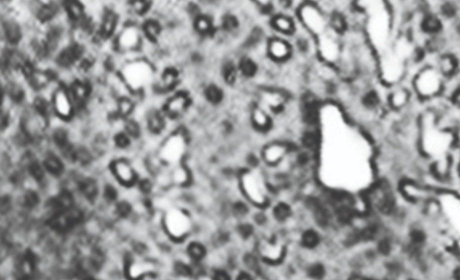
Figure 6: Magnified acoustic view of a small area shows that even tiny voids have bright centers.
When it is critical to characterize a suspected internal structural anomaly as fully as possible, using both x-ray and ultrasound is likely to produce much more comprehensive and diagnosable data. X-ray may miss a very thin but critical gap, but ultrasound will find it. Ultrasound may miss a void that is below multiple interfaces, but x-ray will find it. The combined impact of the two complementary tools on product quality is considerable.


