
Hitachi High-Technologies launch advanced high voltage CD-SEM
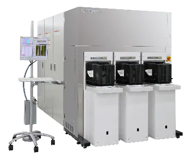
Advanced High Voltage CD-SEM "CV6300 Series" (Image)
Hitachi High-Technologies Corporation announced last month the Advanced High Voltage CD-SEM “CV6300 Series”. CV6300 is the successor of the CV5000 Series, and enables measurements of high aspect ratio*1 deep holes and trench bottom dimensions to control the manufacturing of 96 layers or higher 3D-NAND flash memory*2, as well as high-speed and high-precision overlay*3 measurements. The CV6300 Series will contribute to productivity improvements in semiconductor device manufacturing.
In addition to the miniaturization that has been improving the performance of semiconductor devices, there has been accelerated progress to make the device structures three-dimensional. For 3D-NAND state-of-the-art flash memory device, memory capacity is being expanded by stacking multiple memory cells vertically, and multi-layering technology is advanced from the current 64 layers structure to 96 layers or 128 layers. To control the size and shape of memory cells in the manufacturing process, it is necessary to precisely measure the bottom dimensions of memory holes and slits (trenches), which have become deeper due to the increased multi-layering. For the manufacturing of DRAM*4 and logic devices, there are requests for more accurate alignment between upper and lower device patterns alongside the advances in miniaturization. For this reason, high-precision fast overlay measurements at many points across the device are becoming a necessity.
The newly-developed CV6300 Series is the world's first*5 advanced in-line measurement system that realized a 45kV acceleration voltage. The maximum acceleration voltage of the irradiating electron beam (primary electron beam) has been increased from 30kV in the previous CV5000 Series to 45kV, with a significant increase of the signal amount of the reflected electrons (BSE*6) generated by the interaction of the primary electron beam and the test sample. This allows to achieve a high-resolution high-quality imaging, and enables highly accurate measurements of deep holes and trench bottom dimensions. In addition, by improving the precision of adjustments and stability of the primary electron beam, Hitachi High-Tech has achieved precision improvement in dimensions and overlay measurements, as well as a reduction of measurement variation among systems. Furthermore, due to the adoption of new wafer stage and optimization of dimension measurement sequencing*7, measurement throughput has been improved by about 25% compared to the previous model.
Hitachi High-Tech will strive to meet customers’ needs in dimensions measurements and defect inspection for the development and mass production of semiconductor devices by supplying electron beam based products such as traditional CD-SEM, High voltage CV6300 Series, and wafer inspection systems based on optical technologies. Hitachi High-Tech will continue to provide innovative solutions for upcoming technology challenges. In parallel, Hitachi High-Tech will contribute to cutting-edge technologies by pursuing and creating new value in collaboration with its customers.


