
Fingerprinting analysis on electronic materials
As semiconductor device geometries continue to shrink, electronic materials are increasingly critical to reducing defects while ensuring high yields. The experts at Linde describe the extraordinary lengths they pursue to ensure purity, quality and consistency.
By Carl Jackson, Head of Electronics R&D, Linde
“You can’t manage what you can’t measure” is an often-quoted business mantra developed in the 1950s by the prominent operational management thinkers of the time, the same era as the start of the semiconductor age. Peter Drucker was one of the key proponents of this new approach referring to the increasing need for objective data to improve business processes. In semiconductor manufacturing, this approach has been taken to the extreme, allowing the industry to shrink transistors one million-fold in size through a cycle of measurement, innovation, and refinement. But in the current age of exponential data growth, knowing which data are important and how to combine different data sources to get the necessary information for decisions is critical. In this article, we describe how we at Linde have taken an advanced, holistic approach to chemical metrology for electronics materials which we call fingerprinting. As the quality gatekeepers between industrial chemical sources and zero-defect atomic-scale manufacturing, we demonstrate the application of these advanced methods throughout the electronic materials supply chain with real production examples.
Electronics materials: semiconductor building blocks sourced from the chemical industry
Electronic materials are the molecular building blocks used for semiconductor manufacturing. These materials are critical to all semiconductor manufacturing processes (Figure 1, refer to page 8), and are often cited by leading-edge companies and OEMs as one of the key enablers to drive future innovation. Many of the materials in use today – such as silane, ammonia, and hydrochloric acid – have been used since the start of the semiconductor industry, and the purity requirement for these materials has tightened as transistor sizes have shrunk. There are also many new materials like gallium and antimony sources being quickly developed and introduced in response to the increasing challenges of our customers to make electronics devices faster, lower-power or lower-cost. Before any new material can be introduced into manufacturing, metrology must be developed for its entire supply chain.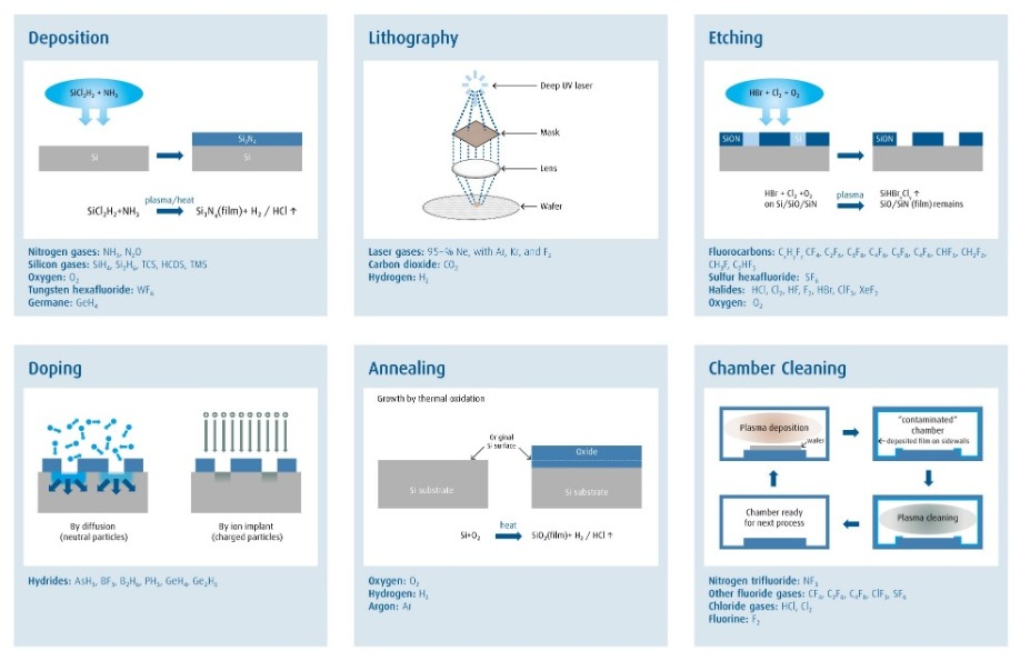
Figure 1: A wide portfolio of electronic materials are used in every major semiconductor process.
Almost all these materials originate from industrial or mined sources instead of being specifically synthesized for use in electronics. This supply is driven by the cost advantage of manufacturing scale. As seen in Figure 2 (refer to page 9), the industrial supply for common materials dwarfs the electronics demand. However, there is a large quality gap between most industrial applications and semiconductor manufacturing. The challenge for electronic material suppliers is identifying stable sources, working with suppliers to understand our sector’s control requirements, and purifying and packaging the materials for use in electronics fabs. Underwriting this supply chain are analytical measurements at each step.
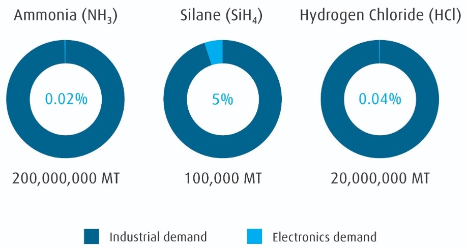
Figure 2: Global electronic material demand is a small fraction of industrial production.
Chemical analysis is the lead metric for ensuring semiconductor-grade quality materials
Long before Peter Drucker’s contributions to business management, nineteenth century scientist Lord Kelvin expounded “to measure is to know.” Chemical analysis and chemical science have developed together, one enabling the other. Early analytical techniques for electronic materials focused on a few impurities from ambient contamination, namely moisture, oxygen, and particles. These are normally measured by analyzers designed to measure a single impurity.
As process flows became more complex, measurement of a greater number of impurities was essential to characterize and control electronic materials. Spectral techniques which can identify and measure many different species are now typically used. The three most important of these techniques are introduced in Figure 3 (refer to page 10), along with examples of their methods for fingerprinting distinguising between two simple and similar impurities. 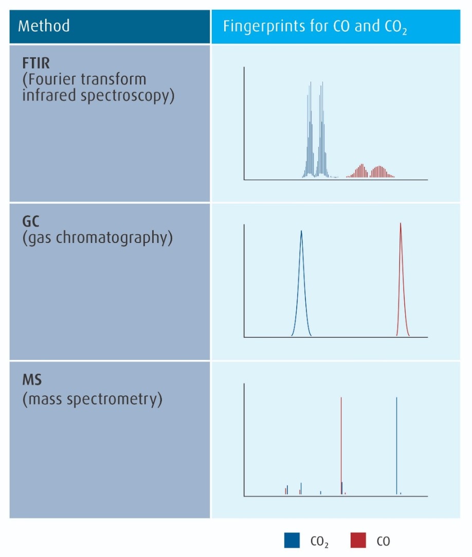
Figure 3: The three most common spectral methods for electronic material analysis, with examples of their fingerprints for carbon monoxide (CO) from carbon dioxide (CO2).
In all electronic materials, many different impurities may be simultaneously present, with most in very minute amounts, even by our industry’s standards. Typically, a subset of the most prevalent or impactful impurities are measured as metrics for both upstream supply chain control and downstream process control. These constitute an agreed specification for the material, and each package or batch of materials is shipped with a list of these measurements called a certificate of analysis, or CoA.
Recently, electronic material suppliers have worked cooperatively with leading-edge device manufacturers to enhance the feedback loop for quality control. Ship-to-control describes the improvement quality feedback loop in which the statistical variation of product impurities and other metrics are continuously evaluated and improved, resulting in quality beyond the CoA specification and a higher-value material product.
Fingerprinting: compiling the data
Fingerprinting is a broad-spectrum chemical analysis which utilizes a collection of instrumentation and analytical techniques to provide a complete characterization or fingerprint of a material. It is not limited to impurities specified on the CoA or even known impurities. Rather, it utilizes spectral techniques like FTIR (Fourier-transform infrared spectroscopy), GC (gas chromatography) and MS (mass spectrometry) which can simultaneously detect a wide range of impurities, in combination with other measurements, to make a comprehensive profile for a material.
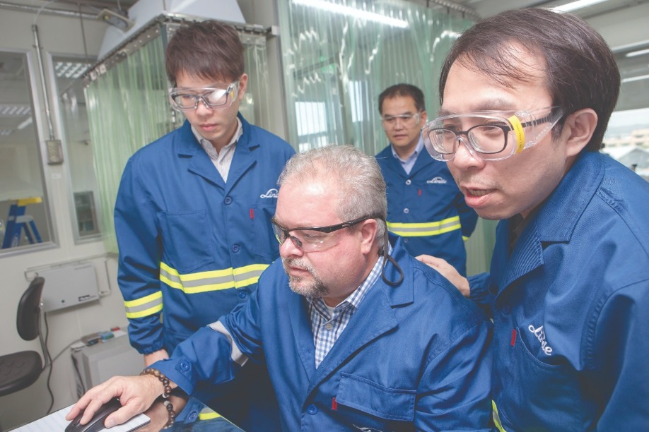
Linde analytical chemists discuss results
Fingerprinting is particularly powerful for impurities which may be detected, but not fully identified or characterized. This is becoming more common as complex molecules are introduced into semiconductor manufacturing, and these complex materials have similarly complex impurities. These impurities may not even be stable outside the matrix of the bulk material, and standards may not be available to calibrate their concentration. Using fingerprinting we can detect the relative changes in the overall composition of a material from different sources, through different points in our manufacturing process, or over time. It allows us to control for multiple variables at the same time, and over all of the points in our supply chain. Fully realized, fingerprinting enables the continuous improvement goal of ship-to-control.
We have been using this approach for many years to help with root-cause analysis when there has been a quality excursion. This has required a bespoke, project-by-project approach where a complex assortment of metrology equipment is required along with the development of new analysis methods.
The recent step-change in our approach is twofold. First, we have established an electronic materials laboratory in Taiwan with capabilities to more efficiently apply fingerprinting on the more than 50 products in our portfolio. The second, more profound change, is that we are now applying the same metrology capabilities not only for complex problem diagnosis, but also for each step in the manufacturing value chain.
Raw material characterization: We can identify and qualify preferred sources of raw materials during our development phases, and we can monitor the quality control of our suppliers with techniques much more powerful than those at the supplier.
*Purification: Chemical analysis guides the development of our purification technologies, and ensures that production lines remain in control and improve over time.
*Analysis: Just as we develop our own purification processes, we also must develop our own analytical methods. Fingerprinting guides us to look at the challenge from many different angles. For production, we can assure our customers that the CoA specification is indicative of our control over the entire profile of the product.
*Packaging, logistics and shelf life: Our responsibility for quality doesn’t end with production, but extends to product stewardship through the packaging, transport, and lifetime of our products.
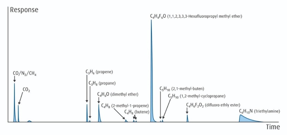
Figure 4: Candidate raw material source for advanced fluorocarbons with a complex mixture of impurities identified by combining GC and MS methods.
Case studies: using data to add value to our materials
Case Study #1: Complex fluorocarbon materials make for challenging sourcing, purification and analysis
Fluorocarbons have long been used as etch materials in electronics manufacturing. When activated by a plasma in an etching tool, chemically active fluoride ions and radicals are produced, which react with many deposition materials to form volatile products which in turn are removed by vacuum pumping. Initially, simpler, more common materials like CF4 and C2F6 were the primary etchants used. Now, more complex materials like C4F6, C4F8, and C5F8 are used to achieve a greater selectivity for preferentially removing one material while leaving a desired second material in place.
The greater complexity of these fluorocarbon materials also means the sources have many more potential impurities, and the purification and analysis become more challenging. Figure 4 (refer to page 11) is indicative of the fingerprint of a potential source material for our process, where we have used a combination of GC and MS techniques to separate and identify the many impurities present. We used fingerprinting to choose and qualify material sources; develop our proprietary purification technology; and to further develop advanced hybrid analytical techniques to ensure ship-to-control quality.
Case Study #2: Carbon monoxide – a simple molecule with extremely low but impactful metal impurities
Carbon monoxide (CO) is also used in etch processes, and is added to further modify the selectivity. The challenge for supplying CO is its reactivity with many common metals, like iron and nickel, to form gas-phase metal-containing compounds called metal carbonyls. Because they are volatile molecules, metal carbonyls can travel unimpeded through particle filters.
Leading-edge processes are extremely sensitive to metallic impurities, and now have a specification of less than 100 parts per trillion (ppt) for both nickel carbonyl and iron carbonyl species. Current detection limits of commercially available analytical instruments do not allow for measurements of carbonyls at the ppt level, and furthermore, the sampling system and analysis instrument itself can react with carbon monoxide to produce carbonyl levels that are higher than in the material being analyzed.
For this reason, we limit our analysis system to non-carbonyl generating wetted materials, which can preferentially capture and concentrate the metal carbonyls. In addition, we have developed state-of-the-art compound methods with both high resolution and high sensitivity to achieve detection and measurement of these species to the low ppt range.
Case Study #3: Silane and the case of the hidden impurities
Silane is the most basic precursor for the deposition of silicon-containing thin films, and has been used for many decades as a workhorse in electronics manufacturing, not only for semiconductors, but also for display and photovoltaic panels. However, even with well-characterized sources and processes, new challenges can arise.
In addition to developing technologies to look at impurity levels that are below current industry practice such as the CO example above, we also have been addressing challenges where the use of standard industry metrology techniques would effectively hide an unknown impurity – a phenomena called matrix interference. Using a variety of analytical techniques with unique overlapping capabilities to look at a wide array of analytes ensures that something hidden by matrix interferences isn’t missed. In the case of silane, GC is the principle analytical technique employed to look for impurities.
However, since some light hydrocarbons have a similar boiling point and vapor pressure curve to silane, they are hard to separate during the purification process. Unfortunately, this also means they are difficult to separate in the GC analysis. In this case, product shipped to our photovoltaic customer met all agreed specifications, but due to an undetected hydrocarbon contamination, the process performance on the customer tool was resulting in a lower panel power output. In response to this issue, we developed a complementary FTIR method for analyzing silane where we could look at the material from a different perspective.
This allowed us to integrate these new measurements with the original GC results and detect the very low levels of hydrocarbon bad actor, which we then subsequently upgraded our purification systems to remove. See Figure 5 for an example of how we were able to identify one of these contaminants.
Case Study #4: Diborane analysis showcases quality control for shipping and storage
Diborane (B2H6) is used both as a source of boron for silicon doping as well as to modify tungsten deposition processes. There are a number of materials used that have the potential to change their composition and purity during shipping and storage. Diborane is one such product that is a critical material for our customers, however can be unstable if not handled correctly, especially if the diborane packages are exposed to high temperatures during transport or storage. The impurities which can be formed are a result of its reaction with itself to form larger compounds called higher boranes, which have more boron and hydrogen atoms. These higher boranes can cause significant customer process issues. Unfortunately, they are very difficult to measure using current state-of-the-art analytical technologies. Adding to the challenge, there are no chemical standards for higher boranes.
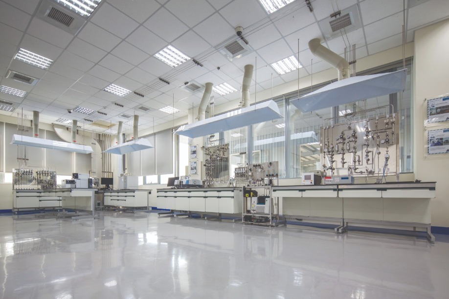
Inside view of Linde Electronics R&D Center analytical laboratory
Working with our customers, we have developed technology to allow us to look directly at part per million (ppm) levels of higher boranes. The traditional approaches with FTIR, GC-FID and GCMS didn’t detect any of the higher boranes that we specifically engineered into the product to simulate a production problem. Instead, we first separated and identified higher boranes in our engineered material using a very advanced combination GC-ICP-MS technique. This technique is powerful, and uses the same inductively coupled plasma technology used in semiconductor deposition and etch processes, but is not always the most consistent and reliable for electronic material production. We then cross-correlated the first results with a more production-robust pure GC technique.
Conclusion: continue to measure and improve
Measure, know, improve. The insights from Lord Kelvin and Drucker continue to guide us and drive us to improve in order to enable our customers’ innovation roadmaps. For the supply of electronics materials, we must bridge a constantly widening gap between industrial raw material sources and ultra-precision atomic level manufacturing. Chemical analysis is our strongest tool to know our products and our processes, and we continuously improve both.
Linde has pioneered the practice of fingerprinting electronic materials. We understand that material development is a critical enabler for our leading customers. By investing and leveraging our world-class analytical production and development facilities in Asia and the US, Linde has focused on high-impact materials for the industry. We continue to invest, develop, and enable technology for the future.
Linde Electronics R&D Center in Taichung, Taiwan


