
VEECO Instruments targets next-gen VCSEL requirements
VCSELs play an increasingly central role in advanced facial recognition applications after years of service in computer peripherals such as mice, scanners and printers. Silicon Semiconductor invited VEECO Instruments to describe key challenges and solutions for increased performance, higher throughput and greater repeatability in VCSEL manufacturing.
Replies from Somit Joshi, VP of MOCVD Marketing and Anil Vijayendran, VP of Precision Surface Processing Marketing, Veeco Instruments
Q: VCSELs (vertical cavity surface emitting lasers) have played a role in computer peripherals for decades and are now central components within facial ID and advanced automotive applications. How did VEECO develop its portfolio and what is new in VCSEL technology?
A: Veeco designs, manufactures and markets thin film process equipment that enables high-tech electronic device R&D and production worldwide, including VCSELs. Since our IPO in 1994, we have delivered advanced packaging lithography, laser annealing, single-wafer etch/clean, ion beam, MOCVD, MBE, ALD and related technologies to solve tough materials engineering challenges for our customers.
Veeco’s expertise and innovations are used in the development and high-volume manufacturing of advanced silicon semiconductor devices for logic and memory applications (e.g., AI, IoT, Cloud Computing); as well as compound semiconductor products for solid-state lighting/displays (e.g., microLED) and power/RF (e.g., pHEMTs for 5G), photonics for 3D sensing (e.g., VSCEL, LiDAR, Augmented Reality) and data communications (e.g., Big Data, autonomous vehicles), to name a few.
In terms of MOCVD, Veeco has been a leader since the year 2000 in the compound semiconductor arena with 100+ man-years of solid domain expertise. Since then, Veeco has released a steady stream of MOCVD systems including the industry leading K475i platforms that have increased capacity and production while lowering cost of ownership. The patented TurboDisc® MOCVD technology is at the core of our capability enabling Veeco’s systems to very precisely apply material to wafers exactly to our customers’ specifications with many inherent advantages.
A VCSEL is a complex compound semiconductor device that’s been around for many years (e.g., in computer peripherals like mice, scanners) and subsequently used primarily in the optical communication in the data and telecom space. More recently (2017 onwards), VCSELs have been applied in the 3D sensing arena (e.g., facial recognition applications, ADAS in driverless vehicles) which will be the main growth driver of the VCSEL industry within the next 5 years.
However, moving from traditional and historical applications to 3D sensing applications adds several challenges related to design and manufacturing. The design challenges include the move to higher power, bigger die size, more cavities and greater precision; all while needing to be integrated into larger modules with complex optics. Manufacturing challenges in VCSELs include the transition to 150mm wafers and more stringent process control for higher reliability and yield requirements in applications like 3D sensing.
Q: How does Veeco Instruments see the market for advanced VCSELs growing, and will this growth be primarily for higher-order devices with greater performance?
A: We expect existing VCSEL use to grow and proliferate into additional applications over the next few years. We anticipate explosive growth for new applications in step with megatrends like AI, VR/AR and autonomous transportation, gesture sensing, augmenting cameras with 3D information, LiDAR arrays for distance ranging, short-haul datacom, materials processing, etc.
Veeco scientists have taken this proven domain expertise and optimized our existing platform for VCSEL manufacturing. We believe we have an advantage in this market because our TurboDisc technology provides the performance requirements without compromising productivity and uptime, resulting in an overall lower cost of ownership. We have demonstrated excellent uniformity and defectivity data using TurboDisc technology with extremely positive customer feedback.
Also, reactor design incorporating Veeco’s Uniform FlowFlange™ technology produces films with very high uniformity and improved within-wafer and wafer-to-wafer repeatability with the industry’s lowest particle generation. The simple design provides ease-of-tuning for fast process optimization and fast tool recovery time after maintenance for the highest productivity for applications such as lighting, solar, laser diodes, VCSELs, pseudomorphic high electron mobility transistors (pHEMTs) and heterojunction bipolar transistors (HBTs). Veeco is closely working with industry leaders in enhancing TurboDisc technology that delivers to tighter requirements for the next wave of more demanding applications–world facing applications for smartphones (and other mobility devices) and LiDAR for mission critical ADAS applications. We have validated (with industry leaders) that the TurboDisc roadmap provides the path to meet their tighter requirements on Oxide Layer composition control, Fabry Perot dip uniformity, etc.
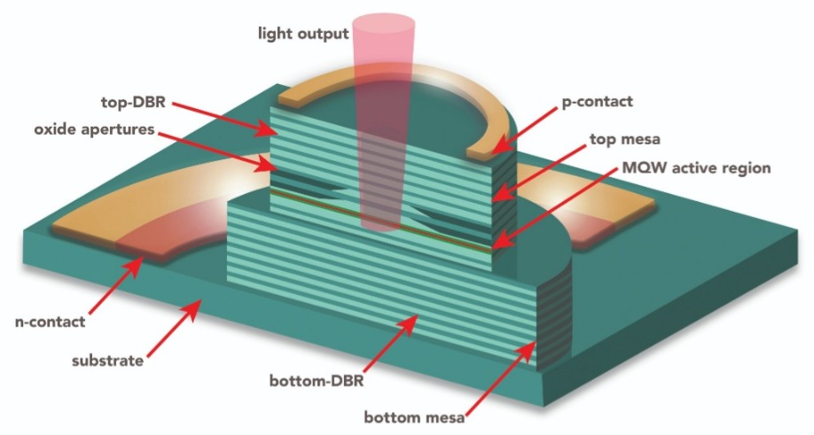
A simplified VCSEL cross-section illustration
Q: Are VCSELs as a product class undergoing fabrication and performance enhancements, and what is essential from Veeco’s perspective for supporting next-generation requirements?
A: Let’s look at the typical steps required to manufacture VCSEL chips: Epitaxy growth, p-side contact, mesa etching #1, passivation, mesa etch #2, and n-side contact. The n-side contact could be a top-side or back-side contact. Note that light emits from the front, while the back may be mounted to a heat spreader for high-power chips.
As mentioned earlier, VCSELs are mainly seen in low-power (few milliwatts) applications for optical data transmission, but higher power (over 100 mW devices emitting at around 980 nm) and higher (implying larger area) are being explored. Problems/challenges as we transition to production include:
High yield for total population in 6 nm bin (for matching with detector optics)
Composition uniformity for aperture size control (defines beam power and divergence)
Low defectivity (< 1/cm2) for structured light and large area VCSELs
Migration to 6-inch wafers from 4-inch
In terms of testing and yield, VCSEL processing (vs. EEL for example) offers cost advantages because testing can be performed while the devices are still in wafer form. Moreover, wafer processing lends itself easily to 2-D array fabrication. Key epi level parameters that directly impact performance and are measured at the wafer level include:
Uniformity (wavelength, composition, sheet resistance)
Linewidth
Defectivity
Power level, threshold voltage, etc.
Most of the manufacturing complexity is in the epitaxial structure and the oxidation process to define the aperture since the remainder of the processing is similar to other compound semiconductor devices such as LEDs, HEMTs, etc. Wavelength control is critical since VCSELs for sensing applications are paired with detectors and narrow band filters. All the die must be within the narrow wavelength window which could be as narrow as 6 nm. Thus, uniformity and repeatability are key. Defectivity control is also important, especially for larger arrays and chips.
The oxidation process sets the aperture size which impacts brightness. The major enhancement is the move to VCSEL arrays, which are large chips, where low defectivity and a uniform aperture are very important so that the performance of each chip in the array is well matched. The multi-quantum-well (MQW) wavelength, FP dip, and DBR stop band must be positioned precisely with respect to each other for the VCSEL to operate efficiently at the rated power.
Several strategies come into play for improving VCSEL performance (e.g. power output, switching speed, efficiency) and reducing manufacturing costs so they can enter more applications. In a VCSEL, the light generated in the active MQW region bounces off highly reflective DBR mirrors on either side of the active region and is partially absorbed as it bounces between the mirrors, while a small portion escapes through the top mirror as the laser beam. Thus, each of these factors must be optimized.
While the epitaxial structure sets the upper bound for the VCSEL performance, real-life performance is based on how closely the epi structure can mimic the targeted design. For example, MQW quality defines the internal quantum efficiency, sharp interfaces in the DBR mirror enhance reflectance, precise positioning of dopants and intrinsically low background doping reduce light absorption and high conductance of the doped regions lowers the series resistance. These in combination set the lasing threshold current, the power conversion efficiency and the linearity of power with current. VCSEL designs for high speed switching require sub 5-micron apertures, strained layers, sharp doping gradients and ultra-thin layers.
Q: What are key cost issues impacting VCSEL production and how can manufactures optimize performance while mitigating cost escalation?
A: Most of the VCSEL manufacturing cost is associated with the epitaxial growth. Achieving consistent performance and high yield through multiple deposition campaigns and across a fleet of tools while maximizing the productivity per chamber (quantified as capex and foot-print efficiency) has the biggest impact on epitaxial manufacturing cost.
This is similar to LED manufacturing, although the manufacturing requirements for VCSELs are much more stringent. Veeco’s TurboDisc technology has proven to be the tool-of-choice that enabled the ramp of LED manufacturing to high volume worldwide. Veeco’s most recent GaN MOCVD system is the EPIK 868, the LED industry’s highest productivity MOCVD system that reduces cost per wafer over 22 percent compared to previous generations.
The LED industry required a cost per lumen reduction roadmap to penetrate a very price-sensitive consumer market, and Veeco’s TurboDisc platform delivered the solutions over time that enabled these targeted reductions on the strength of superior brightness performance and higher uptime and stability.
In fact, Veeco’s historical impact on the LED industry, where over 50 percent of the world’s LEDs were manufactured using Veeco equipment at one point, and the associated energy efficiency and sustainability benefits are often overlooked. Now, TurboDisc technology brings similar productivity and quality benefits to advanced LEDs (for example: microLEDs) and VCSEL manufacturing as the industry positions for the manufacturing ramp. In summary, Veeco is enhancing 6-inch wafer uniformity and controlling Al composition while managing defects and improving doping control by 25-50 percent over the current industry baseline. This is on top of the 40 percent higher productivity provided by TurboDisc technology.
Q: Can you discuss the importance of removing excess photo resist when creating advanced VCSEL devices?
A: In addition to MOCVD equipment, VEECO has world class wet processing systems that are currently used in VCSEL production. For instance, Metal-Lift Off (MLO) is an alternative to dry etching that is used to pattern metal lines. This technique is found most prominently in compound semiconductor applications where metals are not easily etched by plasma. Less expensive than dry etching, MLO relies on the quality of the incoming metal deposition, efficacy of the resist and solvent, and superior system design for success. If during the MLO process, the metal or photo resist is not effectively removed, this will lead to shorting between the lines and yield loss.
The WaferStorm platform with ImmJET technology addresses both technical and productivity challenges. Technically, there is a trend to smaller features which increases the degree of difficulty of removing resist residues. More difficult to remove resists will increase process times and chemical costs. The ImmJET approach of combining batch and single wafer spray combines the best attributes of both technologies. First, the wafer is immersed in solvent for a longer period of time to allow for adequate swelling of resist.
Next, the wafer is moved to a single wafer chamber and the high-pressure spray easily removes the already swelled resist. Veeco’s proprietary software enables the immersion and spray to occur in parallel to enable very high productivity. Innovative filtration and recirculation designs enable low chemical usage and reduced downtime. By enabling superior process control with industry leading throughput and cost of ownership, the WaferStorm and WaferEtch® platforms have achieved process tool of record (PTOR) status at leading customers today.
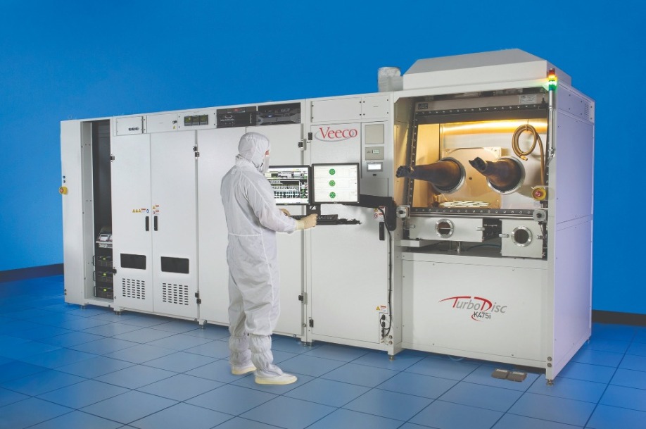
The VEECO Instruments K475i


