+44 (0)24 7671 8970
More publications     •     Advertise with us     •     Contact us
 
News Article

ClassOne Solstice plating system chosen by Taiwanese foundry

News

Solstice will be installed in Yee Wei’s manufacturing facility in Toufen City, Taiwan

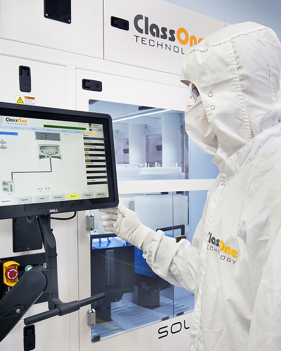
Semiconductor equipment manufacturer ClassOne Technology has announced the sale of its Solstice electroplating system to Yee Wei Co, a semiconductor manufacturing foundry based in Taiwan. The Solstice will be installed in Yee Wei’s manufacturing facility in Toufen City, Taiwan.

“We selected the Solstice for its price-performance and also the range of capabilities it can provide for our 200mm wafer processes,” said Yee Wei President, Chih-Kuang (C.K.) Yang. “The new system features ClassOne’s CopperMax chamber that is optimised for plating copper, which is essential in our advanced R&D processes. The tool also provides a GoldPro™ chamber designed specifically for gold processes, as well as a Vacuum PreWet chamber. Because we are an open R&D fab, the Solstice’s broad flexibility is extremely valuable to us.”

“Solstice is rapidly becoming the de facto standard and process of record for fabs across the world for advanced electroplating production and R&D applications”, said ClassOne CEO, Byron Exarcos, “We continue to gain market share and win in head-to-head situations against competing offerings due to Solstice’s performance, low cost of ownership, and Plating-Plus™ capabilities.”

The Solstice family of wet-processing tools includes the 8-chamber Solstice S8, the 4-chamber Solstice S4 and the 2-chamber Solstice LT. The Solstice platform was specifically designed for ≤200mm wafers, which are used in compound semiconductor, emerging technologies, and numerous other fabs worldwide. The high-performance CopperMax and GoldPro Solstice system configurations have become industry leaders in copper and gold plating as well as in reduced cost of ownership.

Purdue, imec, Indiana announce partnership
Resilinc partners with SEMI on supply chain resilience
NIO and NXP collaborate on 4D imaging radar deployment
Panasonic Industry digitally transforms with Blue Yonder
Global semiconductor sales decrease 8.7%
MIT engineers “grow” atomically thin transistors on top of computer chips
Keysight joins TSMC Open Innovation Platform 3DFabric Alliance
Leti Innovation Days to explore microelectronics’ transformational role
Quantum expansion
indie launches 'breakthrough' 120 GHz radar transceiver
Wafer fab equipment - facing uncertain times?
Renesas expands focus on India
Neuralink selects Takano Wafer Particle Measurement System
Micron reveals committee members
Avoiding unscheduled downtime in with Preventive Vacuum Service
NFC chip market size to surpass US$ 7.6 billion
Fujifilm breaks ground on new €30 million European expansion
Fraunhofer IIS/EAS selects Achronix embedded FPGAs
Siemens announces certifications for TSMC’s latest processes
EU Chips Act triggers further €7.4bn investment
ASE recognised for excellence by Texas Instruments
Atomera signs license agreement with STMicroelectronics
Gartner forecasts worldwide semiconductor revenue to decline 11% in 2023
CHIPS for America outlines vision for the National Semiconductor Technology Center
TSMC showcases new technology developments
Alphawave Semi showcases 3nm connectivity solutions
Greene Tweed to open new facility in Korea
Infineon enables next-generation automotive E/E architectures
Global AFM market to reach $861.5 million
Cepton expands proprietary chipset
Semtech adds two industry veterans to board of directors
Specialty gas expansion
×
Search the news archive

To close this popup you can press escape or click the close icon.
Logo
×
Logo
×
Register - Step 1

You may choose to subscribe to the Silicon Semiconductor Magazine, the Silicon Semiconductor Newsletter, or both. You may also request additional information if required, before submitting your application.


Please subscribe me to:


You chose the industry type of "Other"

Please enter the industry that you work in: