
EV Group and DELO partner to expand materials and process capabilities
Partnership at EVG’s NILPhotonics Competence Center to support new materials development for optical sensor manufacturing and facilitate adoption of wafer-level optics for mass markets
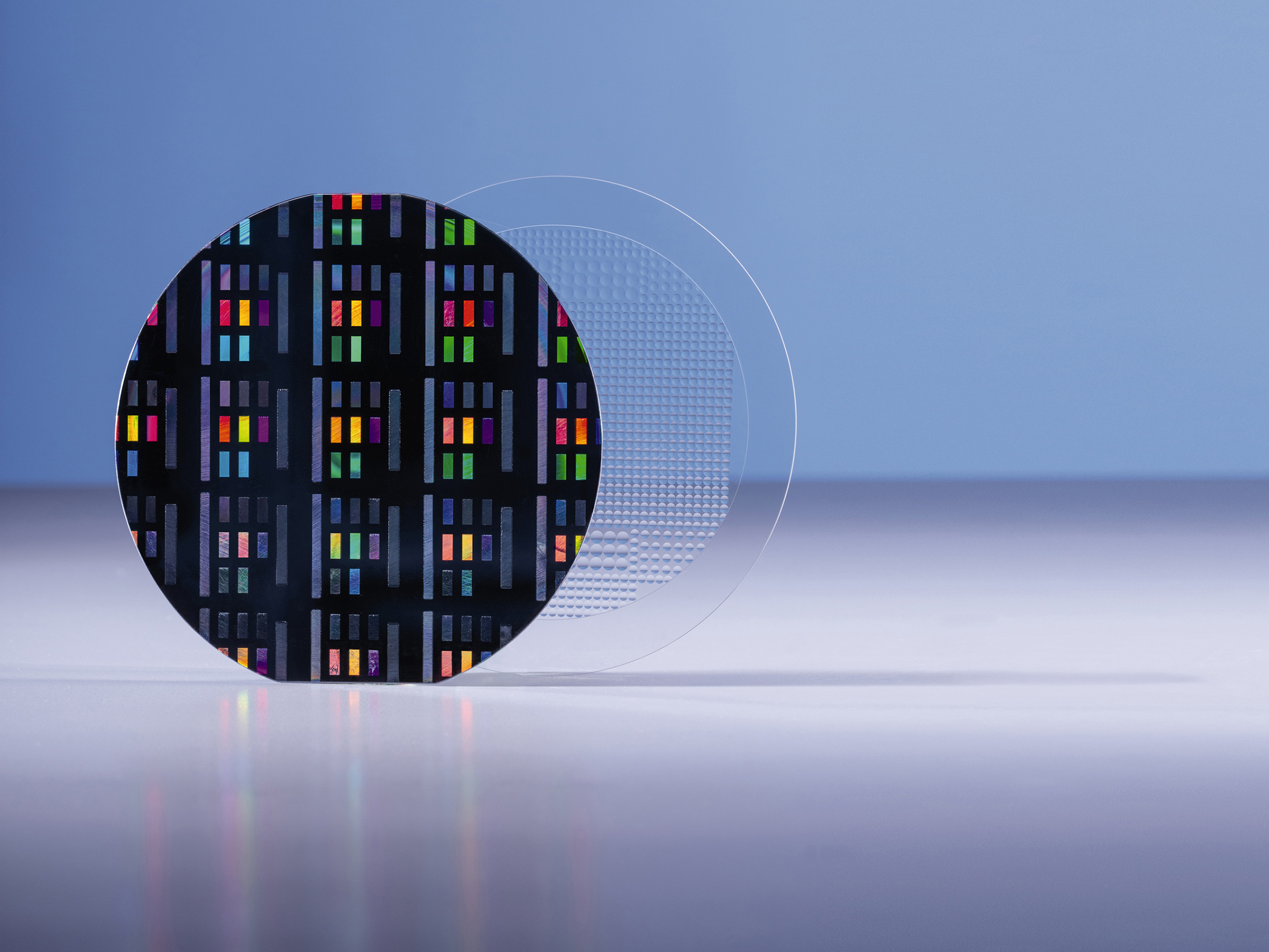
EV Group (EVG), a supplier of wafer bonding and lithography equipment for the MEMS, nanotechnology and semiconductor markets, has announced that it is partnering with DELO, a leading manufacturer of industrial high-tech adhesives, in the area of wafer-level optics (WLO). Both companies, well-known for their leading roles in optical sensor manufacturing, are combining efforts to enable novel optical devices and applications, such as biometric authentication and facial recognition, for the industrial, automotive and consumer electronics markets utilizing EVG’s leading lens molding and nanoimprint lithography (NIL) process equipment and DELO’s advanced adhesives and resist materials.
The partnership, which is being carried out within EVG’s NILPhotonics Competence Center at its headquarters in St. Florian, Austria as well as at DELO’s headquarters in Windach, Germany, will contribute to improving and speeding up material development cycles. EVG’s NILPhotonics Competence Center provides an open access innovation incubator for customers and partners across the NIL supply chain to collaborate to shorten development cycles and time to market for innovative devices and applications. Infrastructure includes state-of-the-art cleanrooms and equipment supporting key NIL manufacturing steps such as step-and-repeat mastering, lens molding and EVG’s SmartNIL® technology, as well as wafer bonding and required metrology. This provides a unique offering to easily access the latest technologies and materials for WLO development, prototyping and manufacturing.
Company executives will be available to discuss this latest joint-development effort at SEMICON Europa, taking place this week at the Messe Munich in Munich, Germany from November 12-15.
Supply Chain Collaborations Driving Adoption of Wafer-level Optics
Advanced adhesives and resists play a pivotal role in enabling wafer-level production of next-generation optical sensors for mass markets. The development of advanced optical materials requires extensive characterization of chemical, mechanical and optical properties as well as proven scalability for high-volume manufacturing (HVM). Particular know-how of material requirements for automated molding and demolding processes as well as excellent material compatibility of working NIL stamps and resists are important as they enable optimal WLO performance at the smallest form factors using proven HVM processes.
Close collaboration between materials suppliers and process equipment manufacturers is key to enabling the development and refinement of processes needed to ensure high reliability and manufacturability of WLO for high-quality products. This joint effort between EVG and DELO will support both companies in refining their processes and products, as well as strengthening their expertise to address current and future market requirements. The partnership will also provide mature material and process know-how to speed up new product design and prototyping, supporting the roadmaps of both companies’ customers.
“The NILPhotonics Competence Center uniquely addresses the industry need for new ways to develop products with short time to market and the highest confidentiality,” stated Markus Wimplinger, corporate technology development and IP director at EV Group. “Through partnerships with key players in the supply chain, such as DELO, we can operate even more efficiently as a central point to develop and establish decisive manufacturing steps for new production lines in close collaboration with process and equipment experts.”
“EVG and DELO are known as technology and market leaders in WLO and NIL equipment and, respectively, optical materials, with a proven track record in ramping these technologies and processes into high-volume production,” stated Robert Saller, managing director at DELO. “Together we can provide unique know-how in applying wafer-level processing technology to optical and photonics manufacturing, making EVG an ideal partner in the development of our latest products. This collaboration will in turn help us to serve our customers as an application expert and premium partner.”
Applications and Solutions for Wafer-level Optics
EVG's WLO manufacturing solutions enable a multitude of novel optical sensing devices for mobile consumer electronics products. Key examples include 3D sensing, time of flight, structured light, biometric authentication, facial recognition, iris scan, optical fingerprint, spectral sensing, environmental sensing and infrared imaging. Other applications include automotive lighting, light carpets, heads-up display, in-car sensing and LiDAR as well as medical imaging for endoscopic cameras, ophthalmic applications and surgical robotics. EVG's WLO solutions are supported by the company's NILPhotonics Competence Center. More information about EVG’s WLO solutions can be found at: https://www.evgroup.com/technologies/wafer-level-optics/.
DELO’s innovative, multi-functional materials are found in nearly every smartphone worldwide. The company’s high-tech adhesives excel at functionality and reliability. With additional characteristics depending upon customers’ specific needs, these polymer materials are optimal for industrial environments with short cycle times where the bonding of tiny elements is needed. In addition, DELO UV-LED-curing equipment and dispensing valves offer outstanding reliability. More information can be found at:
https://www.delo-adhesives.com/en/.
EVG at SEMICON Europa
EVG will showcase its suite of WLO manufacturing solutions, including lens molding, lens stacking and SmartNIL, along with its complete suite of wafer bonding, lithography and resist processing solutions, at SEMICON Europa. Attendees interested in learning more can visit EVG at Booth #B1630.


