Plan Optik driving connectivity to the next level

Plan Optik AG, manufacturer of customized wafers from glass, quartz or glass-silicon compound materials launched its new Cu-Interposer technology at SEMICON Europa 2019.
The progressive miniaturization, increasing integration density and requirements for more powerful signal routing create the need for 3D integration. Interposer technologies for rewiring have been developed for efficient communication with high transmission rates in the 3D chip stack or 3D system package. At present, organic interposers are predominantly used for these technologies. Organic interposers can be produced inexpensively, but are no match for the modern and increasing demands on 3D integration and high transfer rates. Through Glass Via Wafers (TGVs) offer a cost-effective alternative to the costly silicon interposer technology. TGV interposers are a promising technology for three-dimensional and high-density hybrid integration. For high-frequency applications and optoelectronic components, insulation layers are integrated and therefore not required compared to silicon technology of IC chips.
But: There is no established solution to produce glass interposers at wafer level, which provides all the required properties for high-frequency applications. For this reason, Plan Optik has developed a new technology to produce interposers with an applied copper layer, which is particularly suitable for high-frequency applications.
Next Generation Interposer
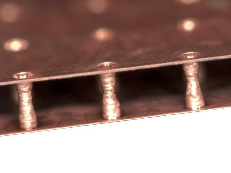
As a first step, Plan Optik will be able to offer Interposers as drilled glass wafers with a copper layer. Those Interposer wafers will be available in sizes up to 300 mm with hole diameters down to 100 µm (depending on wafer thickness). At present, customized Redistribution Layers (RDL) can be integrated on wafer sizes up to 8”. The wafer thickness ranges from 200 µm up to 1 mm. Plan Optik’s Cu-Interposer can be produced as a wafer, as panels or as boards depending on customer needs. With a minimum hole distance equal to via diameter and a Cu-layer thickness starting from 1 µm Cu-Interposer are perfectly suitable for high-frequency applications like for example 5G broadband transmission, radar and imaging sensors, biosensors or beam steering networks.


