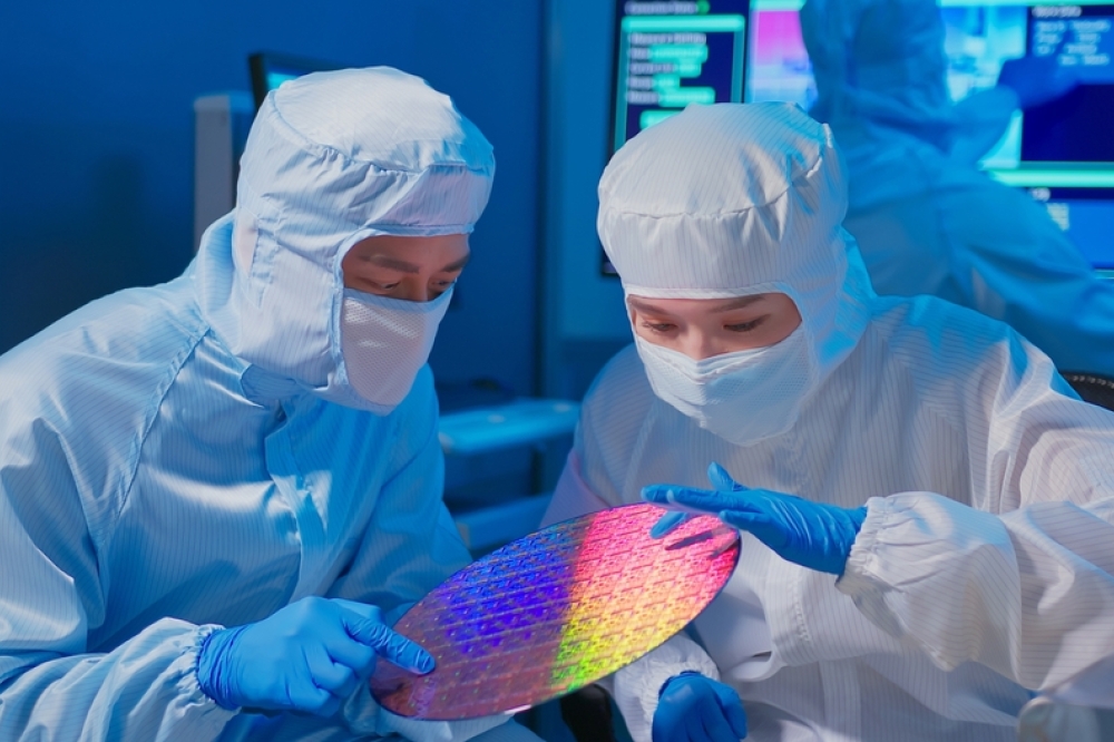
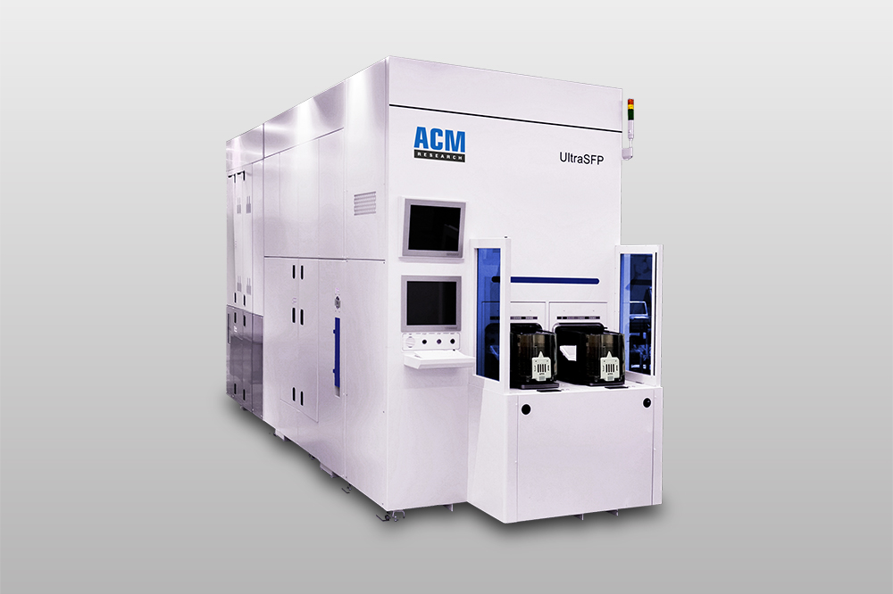
ACM Research Launches Stress-Free Polishing Tool for Advanced Packaging Applications; Delivers First Tool to Leading Chinese OSAT
ACM Research, Inc. a supplier of wafer processing solutions for semiconductor and advanced wafer-level packaging applications, today introduced the Ultra SFP ap tool for advanced packaging solutions. The Ultra SFP ap is designed to address yield issues arising from through-silicon via (TSV) processes and fan-out wafer-level packaging (FOWLP), such as copper overburden post-TSV fill and wafer warpage issues that plague FOWLP processes.
The Ultra SFP ap leverages ACM’s proven stress-free polishing (SFP) technology and integrates it with chemical mechanical planarization (CMP) and wet-etch chambers into a single system. The process wafer moves through the chambers in a three-step approach to gently remove copper overburden and relieve wafer warpage before final planarization and wet-etch steps. Additionally, with its built-in electrolyte recycle and reuse system, the SFP ap consumes significantly reduced levels of chemicals, making it a more sustainable and environmentally friendly option at a lower cost of ownership.
“We completed the research and development for SFP technology in 2009, understanding that it was ahead of its time,” explained David Wang, CEO of ACM Research. “Rapid growth in TSV and FOWLP applications, combined with the push for environmentally friendlier processes at a lower cost of ownership and lower cost of consumables, has provided us with the ideal market conditions to introduce the Ultra SFP ap today.”
ACM also announced today that it delivered the first Ultra SFP ap to a leading Chinese wafer-level packaging provider during the fourth quarter of 2019. This first tool is being verified on the research and development line of this outsourced semiconductor assembly and test customer, with the first round of qualification data expected in mid-2020. The tool will then be moved to the production line for further verification, with revenue recognition upon, and subject to, customer acceptance.
Similar to ACM’s electro-copper plating technology, but in reverse, the Ultra SFP ap’s proprietary electrochemical reaction mechanism involves the simultaneous delivery of electrolytes and a power source to the wafer as it rotates on the chuck to electrically remove metal ions from the wafer surface. In both TSV and fan-out applications, the Ultra SFP ap’s three-step approach effectively eliminates any process-induced stress to the wafer. In TSV applications, SFP is used to remove bulk copper overburden (post-TSV fill) down to 0.2µm. Next, CMP is used to planarize the wafer and remove the remaining copper down to the titanium barrier layer. Finally, a wet-etch step is performed to remove the titanium and expose the oxide layer. In FOWLP, this same sequence of process steps can be used to eliminate wafer warpage, remove copper overburden and planarize redistribution layers.
Because both the electrolyte and wet-etchant chemistries are recycled and reused in real time through a built-in electrolyte recycling system, the Ultra SFP ap can significantly reduce overall usage of consumables. Furthermore, the system’s ability to reclaim the removed metals, which can then be used for other purposes, adds to its sustainable nature.
The Ultra SFP ap 335 is configured with two SFP chambers, one CMP station and two wet-etch/clean chambers. Process chemistries required include electrolytes, copper slurry, copper etchant and titanium etchant. All three processes achieve a 0.5µm/minute removal rate, less than 3% within-wafer nonuniformity and less than 1.5% wafer-to-wafer nonuniformity.