
Imec Demonstrates Si FinFET CMOS devices with Integrated Tungsten Buried Power Rails
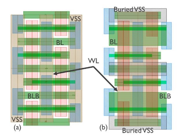
SRAM bit cell (a) without BPR and (b) with BPR.
At the 2020 Symposia on VLSI Technology and Circuits, imec, a leading research and innovation hub in nanoelectronics and digital technologies, presents a tungsten (W) buried power rail (BPR) integration scheme in a FinFET CMOS test vehicle, which does not adversely impact the CMOS device characteristics. When interfacing the BPR with Ru M0A lines through a Ru via contact, excellent resistance values and electromigration behavior have been measured. A complementary assessment study shows the advantages at system level of implementing BPRs as a scaling booster in 3 nm SRAM designs.
Buried power rails (BPRs) have recently emerged as an attractive structural scaling booster allowing a further reduction of standard cell height in highly scaled technologies. Power rails, which are part of the power delivery network, are traditionally implemented in the chip’s back-end-of-line (BEOL, i.e., the Mint and M1 layers). BPRs on the contrary are buried in the chip’s front-end-of-line (FEOL) to help free up routing resources for the interconnects. Moreover, they provide a lower resistive local distribution of the current to a technology that suffers from increasing BEOL resistance with pitch scaling.
Integrating BPRs within the front-end module is however challenging, as BPR processing may induce stress in the conduction channel – degrading the device mobility – or cause metal contamination issues. Imec has experimentally demonstrated the feasibility of integrating W-BPRs in a FinFET test vehicle. Naoto Horiguchi, Program Director CMOS device technology at imec: “Stress transfer could be minimized by burying the W-BPR below the fin, deep into the shallow trench isolation (STI) module. The BPR metal and dielectric were capped by dielectric until the end of the processing. The proximity and processing of the BPR did not impact FinFET device performance, findings that are consistent with 2D stress TCAD simulations, and metal contamination issues were avoided.”
In addition, excellent resistance and electromigration results were obtained after interfacing the W-BPR with a Ru via (Ru VBPR) to contact with Ru M0A lines. “For a W line with critical dimension of 24 nm and length 100µm, no electromigration failures were observed after 900 hours at 330°C and 4 MA/cm2 current density,” commented Naoto Horiguchi.
Earlier studies already showed the essential role of BPRs as a scaling booster in future logic architectures containing nanosheets, forksheets and CFETs. In a complementary study presented at VLSI 2020, imec also evaluated the impact at system level of implementing BPRs in 3 nm SRAM designs. It was shown that burying the VDD and VSS power lines in the SRAM front-end can significantly improve SRAM performance at 3 nm technology nodes. Julien Ryckaert, Program Director Logic insite at imec: “When scaling SRAMs, the grid-like distribution of VDD, VSS, wordlines and bitlines suffers from routing congestion and resistance degradation. This resistance degradation is worst for the wordline. Moving the VDD and VSS power lines below the device – and as such relaxing the dimensions of word- and bitline – can offer a significant performance boost at system level, mainly improving write margin and read speed. For example, our simulations showed a 28.2% performance improvement for a server-processor having BPR-SRAMs with respect to conventional SRAM bit cells in L2 and L3 cache.”

Full front-end-of-line process flow with buried power rail.

Transmission electron microscopy (TEM) showing integrated W-BPR lines with Si FinFET at fin pitch: 45nm. Minimum distance of BPR to fin = 6nm.


