
OLED Rising Market Marks New Era in Lighting and Screen Technology
The OLED panel market is forecasted to grow at a CAGR of 12.9% during 2020-2025 to reach 45.55 billion units by 2025. While there will be a slight downturn overall due to Covid-19 pandemic, industry experts continue to expect OLED panels to be a significant display technology trend adopted across the world, with larger screen sizes, improved 8K resolution and new form factors.
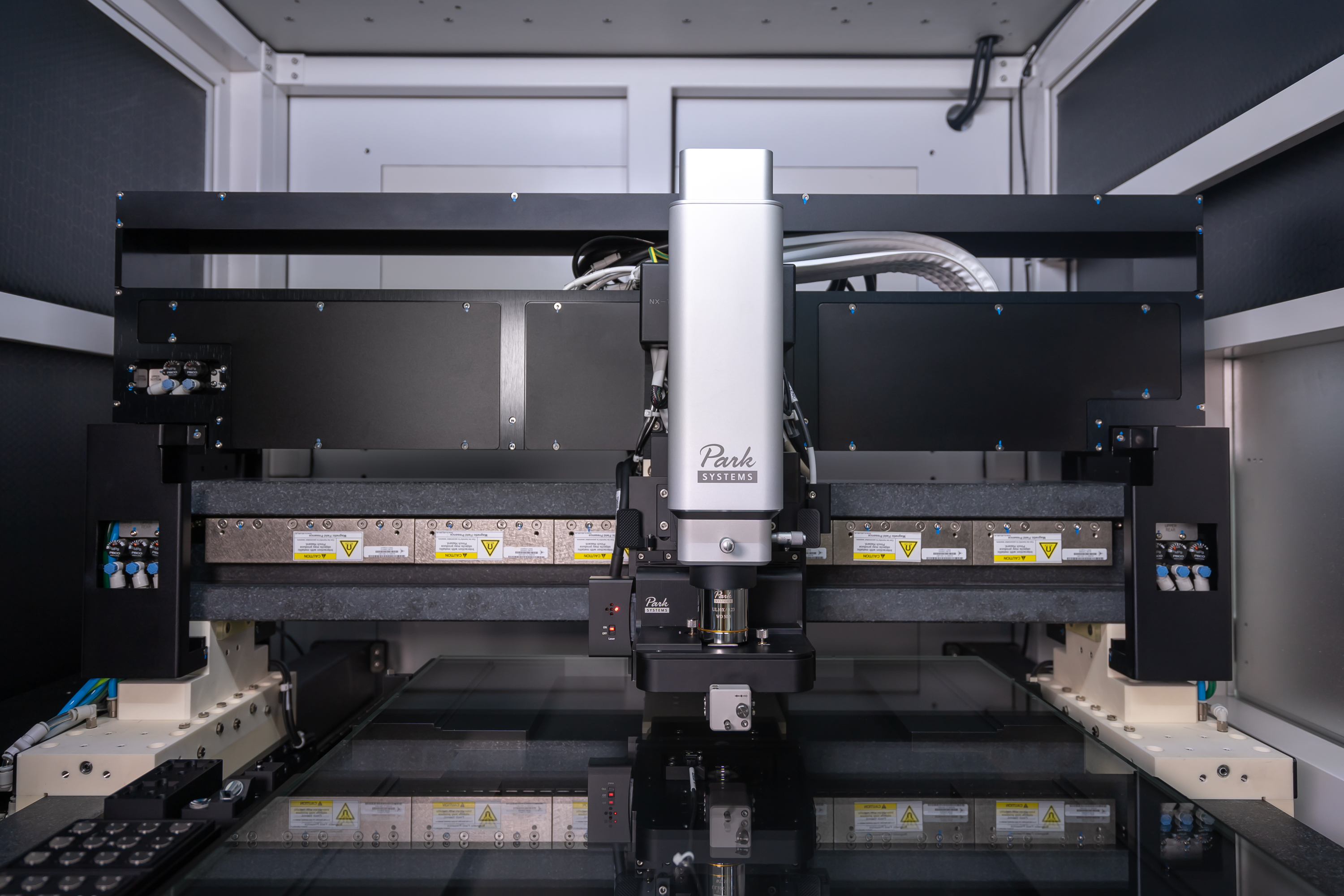
Atomic Force Microscope manufacturer, Park Systems has scaled up its AFM tools for Gen8+ and all large flat-panel displays with the Park NX-TSH (Tip Scanning Head) system. It is the industry’s only automated Tip Scan Head for analyzing samples larger than 300 mm. “Park NX-TSH is designed for large and heavy flat-panel display glass and 2D encoders, with integrated micro probe stations for conductive AFM and electric defect analysis,” explains Keibock Lee, Park Systems President. “Park NX-TSH can scan up to 100 µm x 100 μm (x-y direction) and 15 μm (z direction), and it has a flexible chuck to accommodate samples larger than 300 mm and heavier than 1 Kg—engineered for OLED, LCD and other large sample analysis.”
The Organic Light Emitting Diode Technology
Organic Light Emitting Diode (OLED) technology is being used in an increasing number of application areas because they can be flat, paper-thin and flexible, and have the ability to diffuse light, which is expected to significantly drive the market growth over the next few years.
Park Systems, in anticipation of the market expansion, has developed Park NX-TSH specifically for manufacturers setting up fabs that produce next-generation flat-panel displays with the objective of overcoming the 300 mm sample size limit. Using conductive AFM, Park NX-TSH can measure the sample’s electrical properties by supplying current through the optional probe stations.
The enabling technology for Park NX-TSH is the tip scanning head attached to the gantry that moves to the desired measurement positions on the surface of the sample that is fixed on a sample chuck. The Park NX-TSH tip scanning head system therefore overcomes the limitations of sample size and weight.
OLEDs -A Sustainable Solution for Lighting
OLEDs, the next advance in lighting, differ from LEDs in that the semiconductors used to convert electricity into light are not synthetic single crystals but rather films composed of organic molecules. The organic component makes them lighter and more energy efficient. Large panels can be assembled and stretched into unique displays, enhancing architectural design. Furthermore, it is even more sustainable given that OLEDs do not contain mercury, so when in widespread use they can save enormous amounts of hazardous waste.
To learn more about Park NX-TSH see this video: https://drive.google.com/file/d/19JXpLZYcS9M04lNAe9fYXUiMKmM2Eie4/view
For more information, please visit www.parksystems.com/nx-tsh or email us at inquiry@parksystems.com.


