
ACM Research Launches 18-Chamber Single-Wafer Cleaning Tool
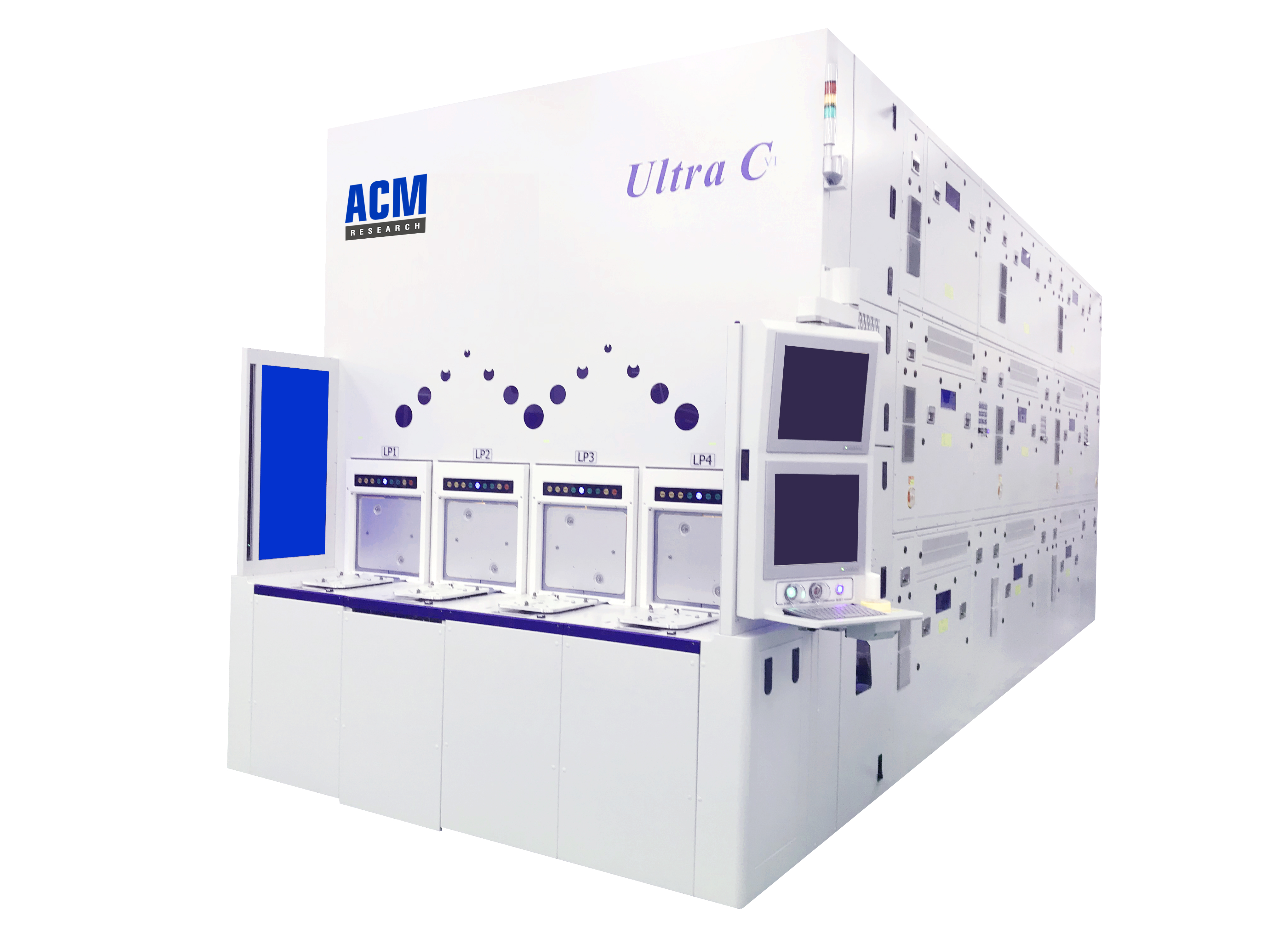
ACM Research, Inc, a supplier of wafer cleaning technologies for advanced semiconductor devices,has announced from SEMICON China its Ultra C VI single wafer tool, the newest addition to its line of Ultra C cleaning systems. The Ultra C VI targets high-throughput cleaning of dynamic random-access memory (DRAM) and 3D NAND Flash devices to support increased production scale. Building on ACM’s proven multi-chamber technology, the new tool features 18 chambers, representing a 50-percent expansion on the throughput and 12 chambers included in the Ultra C V system, with the same tool width and only slightly larger in length to allow for integration into existing production lines.
“Although memory devices are increasing in complexity, they still have the same high throughput requirements,” said ACM’s president and CEO Dr. David Wang. “Additional cleaning chambers enable memory device makers to support extra processing steps and more sophisticated drying technology, while maintaining or reducing production cycle time. We see an 18-chamber configuration as the sweet spot for this application. Compared to systems with higher chamber counts, the Ultra C VI provides a better balance for wafer-per-hour requirements and factory-automation matching.”
The Ultra C VI performs single-wafer cleaning for advanced DRAM devices of 1y nm and beyond, as well as advanced 3D NAND devices with 128 stacked layers and above. It can be used for a variety of front-end-of-line (FEOL) and back-end-of-line (BEOL) processes, depending on the application and the chemistries involved, such as BEOL polymer removal, tungsten- or copper-loop post-cleans, pre-deposition cleans, post-etch and post-chemical mechanical planarization (CMP) cleaning, deep-trench/via cleans, and RCA standard cleans.
Multiple chemical combinations can be used during cleaning, including standard clean (SC1, SC2), hydrofluoric acid (HF), ozonated deionized water (DI-O3), diluted sulfuric peroxide mixture (DSP, DSP+), solvent cleaner, or other process chemicals. Up to two chemicals can be reclaimed and reused, which helps reduce the cost of consumables and overall cost of ownership. The Ultra C VI can accommodate optional physical assistant cleaning methods, such as dual-fluid N2 spray cleaning or ACM’s proprietary SAPS and TEBO megasonic cleaning technologies. It also offers an isopropyl alcohol (IPA) drying function that can be applied to patterned wafers with high aspect ratios. Moreover, as it fits within the same width as ACM’s existing tools, this tool helps improve fab utilization and further contributes to lower cost of ownership.
ACM plans to deliver the Ultra C VI tool to a leading memory manufacturer for evaluation and qualification early in the third quarter of 2020.
To learn more about the complete line of ACM cleaning solutions, including the new Ultra C VI system, please visit ACM in Booth E5223 at SEMICON China, being held June 27-29, 2020, at Shanghai New International Expo Center; or contact the ACM representative for your region listed below.


