+44 (0)24 7671 8970
More publications     •     Advertise with us     •     Contact us
 
News Article

Onto Announces new material analysis tool

News

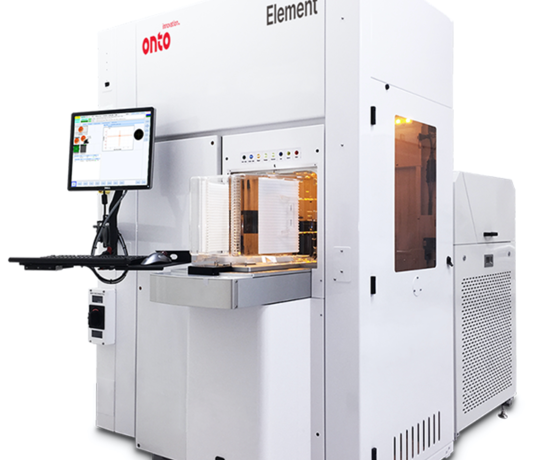
Element Fourier-transform infrared (FTIR) spectroscopy system targets dielectric monitoring of product wafers

Onto Innovation has announced the availability of the Element material analysis platform, which enables customers to monitor and control layers of dielectric thin films, measuring dopants such as boron and phosphorous, as well as monitoring process by-products such as hydrogen. Onto began first deliveries in the second quarter of 2020.

“With the adoption of the Element platform for these new applications, we are moving beyond our existing served available market (SAM) of measuring impurities and epitaxial thickness for the bare silicon wafer market. We believe the inline production monitoring of thin film dielectrics will increase our 2021 SAM by approximately $30 million,” said Robert Fiordalice, vice president and general manager of the Wafer Business Unit.

“Our customers are benefiting from our product output, allowing them to correlate materials characteristics to integration variables like etch selectivity and ultimately parametric yield. We believe the initial orders for the Element FTIR technology indicate a trend for in-line monitoring of materials as the number of dielectrics, and semiconductor materials used in chips is expected to increase exponentially for advanced nodes. Our customer roadmaps indicate a 10X growth in materials monitoring over the next five years.”

Purdue, imec, Indiana announce partnership
Resilinc partners with SEMI on supply chain resilience
NIO and NXP collaborate on 4D imaging radar deployment
Panasonic Industry digitally transforms with Blue Yonder
Global semiconductor sales decrease 8.7%
MIT engineers “grow” atomically thin transistors on top of computer chips
Keysight joins TSMC Open Innovation Platform 3DFabric Alliance
Leti Innovation Days to explore microelectronics’ transformational role
Quantum expansion
indie launches 'breakthrough' 120 GHz radar transceiver
Wafer fab equipment - facing uncertain times?
Renesas expands focus on India
Neuralink selects Takano Wafer Particle Measurement System
Micron reveals committee members
Avoiding unscheduled downtime in with Preventive Vacuum Service
NFC chip market size to surpass US$ 7.6 billion
Fujifilm breaks ground on new €30 million European expansion
Fraunhofer IIS/EAS selects Achronix embedded FPGAs
Siemens announces certifications for TSMC’s latest processes
EU Chips Act triggers further €7.4bn investment
ASE recognised for excellence by Texas Instruments
Atomera signs license agreement with STMicroelectronics
Gartner forecasts worldwide semiconductor revenue to decline 11% in 2023
CHIPS for America outlines vision for the National Semiconductor Technology Center
TSMC showcases new technology developments
Alphawave Semi showcases 3nm connectivity solutions
Greene Tweed to open new facility in Korea
Infineon enables next-generation automotive E/E architectures
Global AFM market to reach $861.5 million
Cepton expands proprietary chipset
Semtech adds two industry veterans to board of directors
Specialty gas expansion
×
Search the news archive

To close this popup you can press escape or click the close icon.
Logo
×
Logo
×
Register - Step 1

You may choose to subscribe to the Silicon Semiconductor Magazine, the Silicon Semiconductor Newsletter, or both. You may also request additional information if required, before submitting your application.


Please subscribe me to:


You chose the industry type of "Other"

Please enter the industry that you work in: