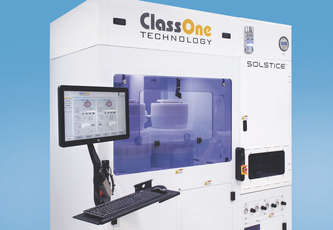
ClassOne’s Solstice LT Plating System Selected by Jenoptik

Semiconductor equipment manufacturer ClassOne Technology announced the sale of its Solstice LT electroplating system to Jenoptik for manufacturing semiconductor material for high-power diode lasers at its semiconductor production facility in Berlin-Adlershof, Germany. High-power diode lasers play an important role in optical pumping of solid-state lasers as well as in direct use applications such as material processing, sensing as well as in healthcare & life science. The dual-chambered Solstice LT is specially configured for high-performance gold processing. The announcement was made jointly by ClassOne CEO, Byron Exarcos, and Dr. Juergen Sebastian, plant manager of the Jenoptik facility in Berlin.
"The new Solstice LT will replace a manual plating wet bench," explained Dr. Sebastian. “This will significantly improve process stability, plating quality as well as reduce our metallization step costs. That’s important because at Jenoptik, we build all the semiconductors that go into our diode lasers in-house. The new Solstice LT electroplating system thus ensures very high quality, performance and service life of our end products. Moreover, the new system also promotes Jenoptik’s policy of sustainability thanks to the new electrolyte technology.”
“The Solstice LT for Jenoptik is specially configured with our GoldPro™ processing chamber,” said Exarcos. “GoldPro can deliver unprecedented levels of repeatability – wafer-to-wafer, die-to-die, within-die, and within-feature. The bottom line is exceptional uniformity and reproducibility, along with reduced cost of ownership.”
With the new electroplating system, Jenoptik is now able to process different GaAs wafers sizes to accommodate different customer requirements. Another reason for selecting Solstice was the flexibility of its design, which readily allows the handling of multiple wafer sizes on the same tool.
“We’re proud to be on the Jenoptik team because their semiconductor lasers are industry leaders,” said Exarcos. “Their quality is based on advanced manufacturing, with strict quality controls and state-of-the-art process technologies. It's an environment in which Solstice can play an integral role, and we're looking forward to the next generations of Jenoptik diode lasers!”
ClassOne Solstice systems provide high-performance electroplating specifically for ≤200mm wafer processing. The Solstice series includes fully-automated 8-chamber and 4-chamber systems with up to 75-wph throughput as well as a 2-chamber semiautomated configuration that can be used both for process development and production. In addition to electroplating, the unique Plating-Plus™ capabilities of the Solstice platform enable it to handle many other important functions, such as wafer cleaning, high-pressure metal lift-off, resist strip, UBM etch, and more. Solstice’s class-leading performance and flexibility consistently make it the tool of choice for ≤200mm plating.


