+44 (0)24 7671 8970
More publications     •     Advertise with us     •     Contact us
 
News Article

SINGULUS receives order from leading semiconductor foundry

News

The semiconductor division of SINGULUS TECHNOLOGIES AG has been awarded an order for a TIMARIS type cluster tool for vacuum deposition on 300 mm wafers. The order in a mid-single-digit range was placed by one of the largest semiconductor foundries of the world and is intended for mass production of integrated inductors.

“We are pleased to convince an additional leading semiconductor foundry with our TIMARIS vacuum deposition platform. Paramount this success was our competence in process development, reliability and productivity of our cluster tools in a state-of-the-art 300 mm Fab”, comments Dr. Stefan Rinck, CEO of SINGULUS TECHNOLOGIES.

Integrated inductors enable highly-integrated voltage regulators. Thin-film transformers convert higher supply voltages to lower operating voltages directly in the chip/package. This has two primary benefits: The considerably smaller footprint allows higher integration in mobile devices. Datacenter benefit from reduced ohmic losses as transformation to higher current takes place at the consumer. SINGULUS TECHNOLOGIES thus enables further integration in the semiconductor industry and the reduction of energy consumption.

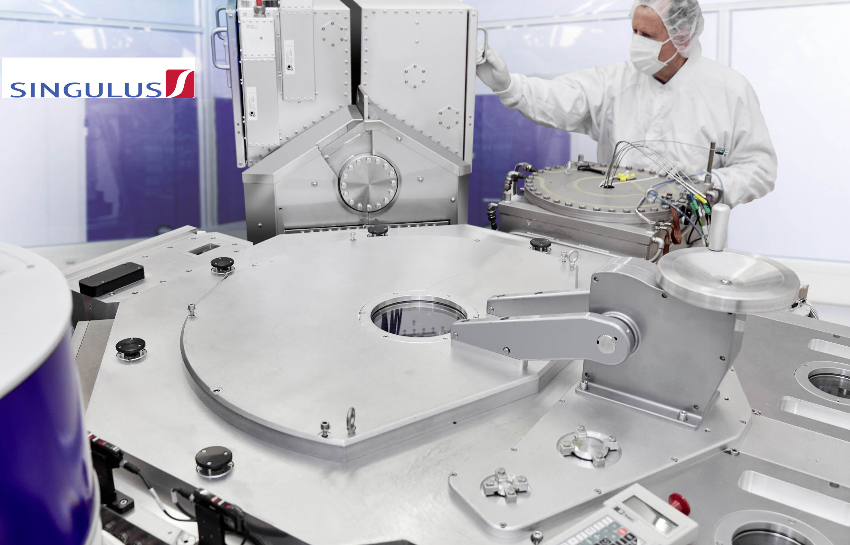
The vacuum deposition cluster tools of the TIMARIS type have modular design and can be equipped with various deposition and auxiliary modules. Amongst others, they include modules for sputtering, which can be equipped with several cathodes and operate in ultra-high vacuum of 10-9 Torr. Furthermore, they seamlessly integrate into the host system of modern, fully automated 300 mm fabs.

Purdue, imec, Indiana announce partnership
Resilinc partners with SEMI on supply chain resilience
NIO and NXP collaborate on 4D imaging radar deployment
Panasonic Industry digitally transforms with Blue Yonder
Global semiconductor sales decrease 8.7%
MIT engineers “grow” atomically thin transistors on top of computer chips
Keysight joins TSMC Open Innovation Platform 3DFabric Alliance
Leti Innovation Days to explore microelectronics’ transformational role
Quantum expansion
indie launches 'breakthrough' 120 GHz radar transceiver
Wafer fab equipment - facing uncertain times?
Renesas expands focus on India
Neuralink selects Takano Wafer Particle Measurement System
Micron reveals committee members
Avoiding unscheduled downtime in with Preventive Vacuum Service
NFC chip market size to surpass US$ 7.6 billion
Fujifilm breaks ground on new €30 million European expansion
Fraunhofer IIS/EAS selects Achronix embedded FPGAs
Siemens announces certifications for TSMC’s latest processes
EU Chips Act triggers further €7.4bn investment
ASE recognised for excellence by Texas Instruments
Atomera signs license agreement with STMicroelectronics
Gartner forecasts worldwide semiconductor revenue to decline 11% in 2023
CHIPS for America outlines vision for the National Semiconductor Technology Center
TSMC showcases new technology developments
Alphawave Semi showcases 3nm connectivity solutions
Greene Tweed to open new facility in Korea
Infineon enables next-generation automotive E/E architectures
Global AFM market to reach $861.5 million
Cepton expands proprietary chipset
Semtech adds two industry veterans to board of directors
Specialty gas expansion
×
Search the news archive

To close this popup you can press escape or click the close icon.
Logo
×
Logo
×
Register - Step 1

You may choose to subscribe to the Silicon Semiconductor Magazine, the Silicon Semiconductor Newsletter, or both. You may also request additional information if required, before submitting your application.


Please subscribe me to:


You chose the industry type of "Other"

Please enter the industry that you work in: