+44 (0)24 7671 8970
More publications     •     Advertise with us     •     Contact us
 
News Article

TEL Introduces Episode UL as the Next Generation Etch Platform

News

Tokyo Electron (TEL) has announced the launch of Episode UL, the company’s next generation etch platform.

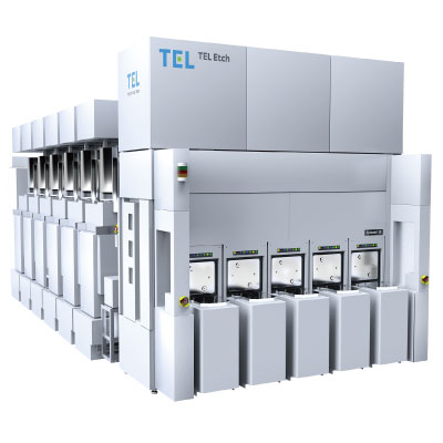
Designed to boost TEL customers’ fab productivity, Episode UL offers many advantages including flexible multi-chamber configurations, significant saving in footprint, ease of maintenance, and advanced Smart tool features.

TEL is the pioneer of space-saving systems with a rectangular cluster design, in which processing chambers are arranged in two horizontally opposed rows. Episode UL can flexibly accommodate between 4 and 12 chambers to maximize loading capacity based on customer fab layouts. With maximum 12 chambers configuration, the new platform’s horizontally opposed cluster design offers significant reduction in footprint per chamber for both cleanroom and utility areas. Episode UL also has a larger space for easier maintenance than that of its predecessors, ensuring greater ease of maintenance. Its transfer system and process modules are equipped with a number of sensors and high-speed control systems, enabling autonomous process control via big data analytics powered by TEL’s proprietary smart tool technology.

“Episode UL embodies the latest advancements in chip scaling and tool intelligence technologies,” said Isamu Wakui, Vice President & General Manager of ES BU at TEL. “This is a technology solution that can significantly improve our customers’ fab productivity. We will continue to develop new technologies and augment our product line-up to meet the ever-intensifying challenges ahead.”

Please use the following link to watch promotion video of TEL Episode UL.

URL: https://youtu.be/OuzSCyUafuE

Purdue, imec, Indiana announce partnership
Resilinc partners with SEMI on supply chain resilience
NIO and NXP collaborate on 4D imaging radar deployment
Panasonic Industry digitally transforms with Blue Yonder
Global semiconductor sales decrease 8.7%
MIT engineers “grow” atomically thin transistors on top of computer chips
Keysight joins TSMC Open Innovation Platform 3DFabric Alliance
Leti Innovation Days to explore microelectronics’ transformational role
Quantum expansion
indie launches 'breakthrough' 120 GHz radar transceiver
Wafer fab equipment - facing uncertain times?
Renesas expands focus on India
Neuralink selects Takano Wafer Particle Measurement System
Micron reveals committee members
Avoiding unscheduled downtime in with Preventive Vacuum Service
NFC chip market size to surpass US$ 7.6 billion
Fujifilm breaks ground on new €30 million European expansion
Fraunhofer IIS/EAS selects Achronix embedded FPGAs
Siemens announces certifications for TSMC’s latest processes
EU Chips Act triggers further €7.4bn investment
ASE recognised for excellence by Texas Instruments
Atomera signs license agreement with STMicroelectronics
Gartner forecasts worldwide semiconductor revenue to decline 11% in 2023
CHIPS for America outlines vision for the National Semiconductor Technology Center
TSMC showcases new technology developments
Alphawave Semi showcases 3nm connectivity solutions
Greene Tweed to open new facility in Korea
Infineon enables next-generation automotive E/E architectures
Global AFM market to reach $861.5 million
Cepton expands proprietary chipset
Semtech adds two industry veterans to board of directors
Specialty gas expansion
×
Search the news archive

To close this popup you can press escape or click the close icon.
Logo
×
Logo
×
Register - Step 1

You may choose to subscribe to the Silicon Semiconductor Magazine, the Silicon Semiconductor Newsletter, or both. You may also request additional information if required, before submitting your application.


Please subscribe me to:


You chose the industry type of "Other"

Please enter the industry that you work in: