TEL Announces Single Wafer Cleaning System

Tokyo Electron (TEL) has announced the launch of the CELLESTA™ SCD single wafer cleaning system, scheduled for release in January 2021.
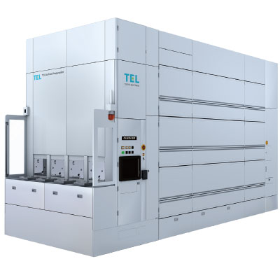
TEL's CELLESTA series of products are widely used for cleaning silicon wafers in the semiconductor manufacturing process. The soon-to-be-released CELLESTA SCD integrates a dedicated supercritical drying chamber on the mass production-proven CELLESTA platform.
In wafer cleaning, it has been customary to employ low surface tension alcohol solutions in the drying process. However, due to continued semiconductor scaling and adoption of multi-layer structures in highly advanced devices, pattern collapse in the drying process has become one major issue. In response, TEL has developed a pattern collapse-free drying method that uses a supercritical fluid, bringing the technology to the market as equipment for mass production.
With the addition of CELLESTA SCD and its dramatically improved cleaning and drying technologies to the existing line of single wafer cleaning systems, TEL is meeting advanced technological needs in semiconductor manufacturing to drive further growth of the semiconductor industry.
“CELLESTA SCD offers an innovative technological solution to the wafer-drying challenges in the post cleaning process for manufacturing advanced semiconductor devices,” said Keiichi Akiyama, Vice President & General Manager, CTSPS BU at TEL. “We will continue to leverage our ability to develop innovative technologies and deliver high value-added products, providing optimum solutions for technological issues associated with the most advanced semiconductor devices.”

AngelTech Live III: Join us on 12 April 2021!
AngelTech Live III will be broadcast on 12 April 2021, 10am BST, rebroadcast on 14 April (10am CTT) and 16 April (10am PST) and will feature online versions of the market-leading physical events: CS International and PIC International PLUS a brand new Silicon Semiconductor International Track!
Thanks to the great diversity of the semiconductor industry, we are always chasing new markets and developing a range of exciting technologies.
2021 is no different. Over the last few months interest in deep-UV LEDs has rocketed, due to its capability to disinfect and sanitise areas and combat Covid-19. We shall consider a roadmap for this device, along with technologies for boosting its output.
We shall also look at microLEDs, a display with many wonderful attributes, identifying processes for handling the mass transfer of tiny emitters that hold the key to commercialisation of this technology.
We shall also discuss electrification of transportation, underpinned by wide bandgap power electronics and supported by blue lasers that are ideal for processing copper.
Additional areas we will cover include the development of GaN ICs, to improve the reach of power electronics; the great strides that have been made with gallium oxide; and a look at new materials, such as cubic GaN and AlScN.
Having attracted 1500 delegates over the last 2 online summits, the 3rd event promises to be even bigger and better – with 3 interactive sessions over 1 day and will once again prove to be a key event across the semiconductor and photonic integrated circuits calendar.
So make sure you sign up today and discover the latest cutting edge developments across the compound semiconductor and integrated photonics value chain.
REGISTER FOR FREE
VIEW SESSIONS