
South Korean Point Engineering Chooses ClassOne’s Solstice S8 for Advanced Semiconductor Plating
ClassOne Technology, global supplier of high-performance semiconductor electroplating and surface preparation systems, announced the sale of its Solstice S8 system to South Korean chip manufacturer, Point Engineering Co. The eight-chambered Solstice plating tool will be installed at Point Engineering’s manufacturing facility in Asan City, South Korea. The announcement was made by ClassOne‘s CEO, Byron Exarcos, and PEC‘s CEO, Bum-Mo Ahn.
"Our products call for unique manufacturing approaches,” said Bum-Mo. “In addition to copper, we require plating of palladium cobalt alloy into highly variant features; and this plating is done on a proprietary substrate. We needed a volume-manufacturing platform that has the necessary flexibility without sacrificing reliability. The Solstice S8 covers these needs very well, and it also has a compact footprint to conserve fab space."
Exarcos pointed out that Point Engineering's new Solstice configuration includes a CopperMax processing chamber, a ClassOne-proprietary feature specifically designed to optimize copper plating. The chamber enables consistent high-quality, high-rate copper plating, while maximizing uptime and dramatically reducing bottom-line operating costs.
“Point Engineering has gained considerable respect in the industry for its semiconductor parts, which frequently go into probe pins and micro power inductors," said Exarcos. “In today’s semiconductor industry, we’re seeing that new product categories often drive the need for novel approaches in manufacturing. Point Engineering’s groundbreaking new products demand a process-experienced equipment provider and a flexible platform. We’re gratified that Point Engineering has chosen ClassOne and Solstice to partner with them on their next-generation products.
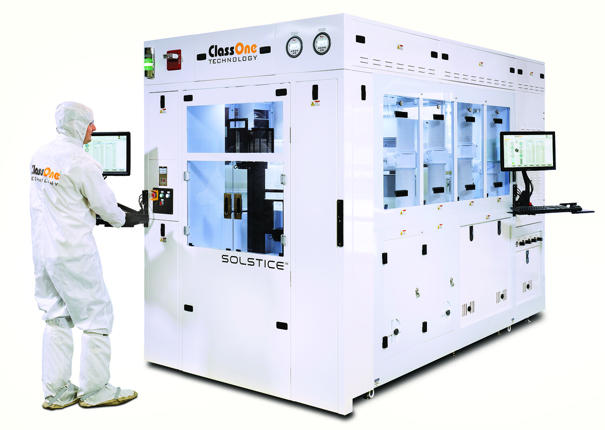
The Solstice S8 is an 8-chambered system designed and built by ClassOne for high-performance, fully-automated electroplating and surface preparation, specifically for ≤200mm semiconductor wafer processing. The Solstice series also includes the S4, which provides up to four processing chambers, and the LT, with up to three chambers. In addition to electroplating, Solstice systems also provide Plating-Plus™ surface preparation capabilities, including wafer cleaning, high-pressure metal lift-off, resist strip, UBM etch and more. This multi-processing flexibility allows users to streamline wafer production and increase cost efficiencies by reducing the number of different processing tools required in the fab.


