
Imec Demonstrates 18nm Pitch Line/Space Patterning
At the 2021 SPIE Advanced Lithography Conference, imec, a leading research and innovation hub in nanoelectronics and digital technologies, demonstrates for the first time the capability of directed self-assembly (DSA) to pattern line/spaces with a pitch as small as 18nm, using a high-chi block copolymer (high-χ BCP) based process under high volume manufacturing (HVM) conditions. An optimized dry-etch chemistry was used to successfully transfer the pattern into an underlying thick SiN layer – which will enable further defectivity inspection. These results confirm the potential of DSA to complement traditional top-down patterning for the industrial fabrication of sub-2nm technology nodes.
The further miniaturization of devices will require the patterning of features that have critical pitches below 20nm. For these small feature sizes, the traditional top-down lithography patterning is increasingly challenged with issues that are inherent to the reaction of the photosensitive materials with light – such as stochastic printing failures and line-edge/line-width roughness (LER/LWR). Since 2010, industry began to take an interest in alternative bottom-up patterning approaches, such as directed self-assembly (DSA), as a potential route to complement and further extend the photolithography-based patterning.
DSA uses the microphase separation of a block copolymer (BCP) to define a pattern. The pattern can be engineered by tuning the composition and size of the polymer. The assembly can be further guided – directed – by using a prepattern of either line/spaces or holes. This results in a final regular nanosized pattern with much tighter pitch (30-5nm) than the guide template. In 2019, imec could generate a pattern of 28nm pitch line/spaces with low and stable defectivity (i.e., bridges and dislocations), based on the DSA of the PS-b-PMMA block copolymer.
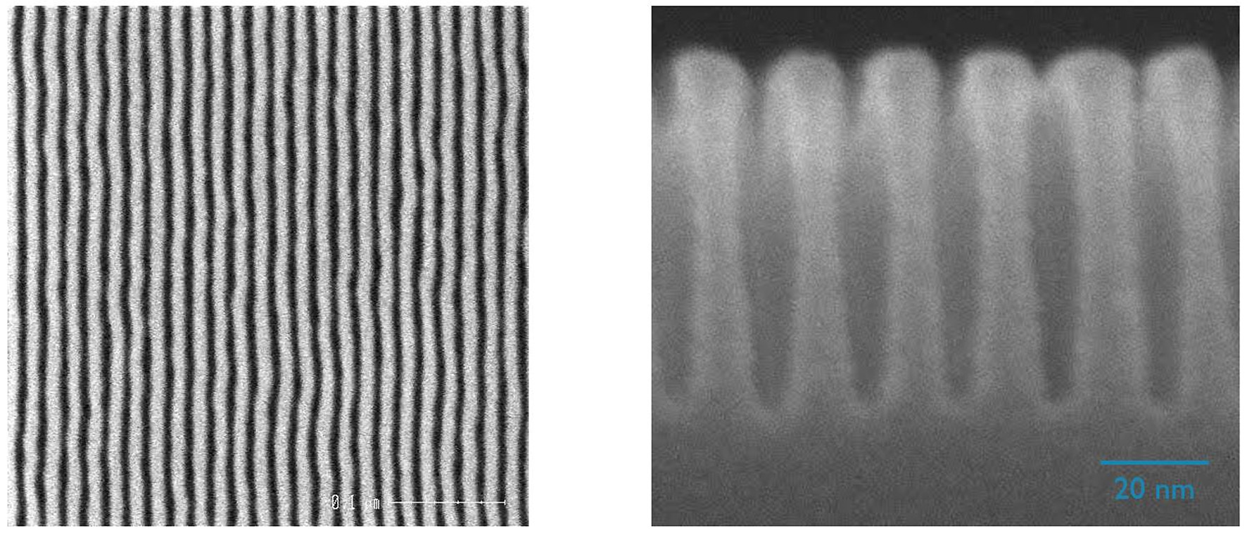
Based on these learnings, imec has now shifted the focus to develop the DSA process towards sub-20nm pitch patterning by using the second-generation block copolymers, i.e., high-χ BCPs from imec’s DSA materials partners (Merck KGaA, Darmstadt, Germany, Brewer Science Inc., Nissan Chemical Corp., Tokyo Ohka Kogyo Co. Ltd.). The pattern was prepared from a 90nm full pitch guide pattern printed by 193 immersion lithography. After 60 second self-assembly of high-χ BCP at HVM-friendly track (SCREEN Semiconductor Solutions Co., Ltd.), no dislocations could be detected from 18nm pitch L/S pattern for the best case. “The subsequent transfer of the high-aspect ratio lines into the underlying material stack was very challenging,” says Hyo Seon Suh, Exploratory Patterning Materials team leader at imec. “As a first step, we etched one block of the BCP by using a dry etch process with optimized etch selectivity. After opening the block, the other block was transferred into the underlying stacks, which served as a hard mask for further patterning a SiN layer. A customized dry etch chemistry, developed in close collaboration with Tokyo Electron Ltd., allowed the 18nm line/space pattern to be successfully transferred into a SiN layer deep enough for following defect inspection, without remarkable line wiggling or line collapse.” In a next phase, this patterned layer will be used to set up the metrology for defectivity inspection and LER/LWR measurements
“In recent years, DSA has attracted large industrial interest which has evolved into a valuable ecosystem of universities, metrologists, material and equipment suppliers. Our DSA ecosystem has been key to the results that we have achieved so far,” says Steven Scheer, VP Advanced Patterning Process and Materials at imec. “For the first time, we showed the capability of DSA to move beyond 20nm pitch for line/spaces. The process is scalable towards smaller pitches by gradually enhancing the BCP’s χ-value. We believe that this bottom-up technique is capable of complementing traditional top-down patterning schemes or be used in combination with EUV lithography for patterning the most critical features of
Top-down (left) and cross-sectional (right) SEM images of an 18nm line/space pattern after high-χ DSA and subsequent etching into a target SiN layer.


