+44 (0)24 7671 8970
More publications     •     Advertise with us     •     Contact us
 
News Article

Tokyo Electron Announces PICP Pro Plasma Etch Systems

News

*PICP: A plasma module that generates highly uniform, high-density plasma on a panel substrate.

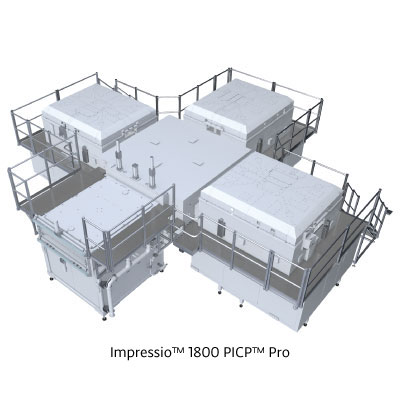
Tokyo Electron (TEL) has announced the launch of Impressio 1800 PICP* Pro and Betelex 1800 PICP Pro, the company’s latest plasma etch systems featuring the new PICP Pro chamber for high resolution processing of 6th generation (G6: 1,500 mm x 1,850 mm) glass substrates.

In the G6 display segment where smartphones are the main application, the wider adoption of high resolution OLED is expanding, and further innovations enabling lower power consumption and smarter user interfaces are eagerly awaited. Such innovative technologies would require densely packed circuit patterns, which calls for more rigorous control capabilities in manufacturing equipment than ever before.

In response to these market demands, TEL has developed PICP Pro, which offers a new capability to control the plasma-space-generating area while retaining the high-precision etch performance of TEL’s proprietary PICP high-density plasma source. The newly added capability reduces the generation of particles that adversely affect maintenance and yield, achieving lower running costs than those for previous PICP.

“PICP Pro is TEL's original development considering our customers’ true needs in their mass-production lines,” said Hiroshi Ishida, FPD Business Unit General Manager at TEL. “PICP Pro offers superior etch precision and higher yield in the advanced display segment.”


Purdue, imec, Indiana announce partnership
Resilinc partners with SEMI on supply chain resilience
NIO and NXP collaborate on 4D imaging radar deployment
Panasonic Industry digitally transforms with Blue Yonder
Global semiconductor sales decrease 8.7%
MIT engineers “grow” atomically thin transistors on top of computer chips
Keysight joins TSMC Open Innovation Platform 3DFabric Alliance
Leti Innovation Days to explore microelectronics’ transformational role
Quantum expansion
indie launches 'breakthrough' 120 GHz radar transceiver
Wafer fab equipment - facing uncertain times?
Renesas expands focus on India
Neuralink selects Takano Wafer Particle Measurement System
Micron reveals committee members
Avoiding unscheduled downtime in with Preventive Vacuum Service
NFC chip market size to surpass US$ 7.6 billion
Fujifilm breaks ground on new €30 million European expansion
Fraunhofer IIS/EAS selects Achronix embedded FPGAs
Siemens announces certifications for TSMC’s latest processes
EU Chips Act triggers further €7.4bn investment
ASE recognised for excellence by Texas Instruments
Atomera signs license agreement with STMicroelectronics
Gartner forecasts worldwide semiconductor revenue to decline 11% in 2023
CHIPS for America outlines vision for the National Semiconductor Technology Center
TSMC showcases new technology developments
Alphawave Semi showcases 3nm connectivity solutions
Greene Tweed to open new facility in Korea
Infineon enables next-generation automotive E/E architectures
Global AFM market to reach $861.5 million
Cepton expands proprietary chipset
Semtech adds two industry veterans to board of directors
Specialty gas expansion
×
Search the news archive

To close this popup you can press escape or click the close icon.
Logo
×
Logo
×
Register - Step 1

You may choose to subscribe to the Silicon Semiconductor Magazine, the Silicon Semiconductor Newsletter, or both. You may also request additional information if required, before submitting your application.


Please subscribe me to:


You chose the industry type of "Other"

Please enter the industry that you work in: