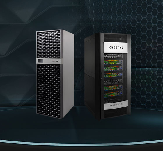
Cadence Unveils Next-Generation Palladium Z2 and Protium X2 Systems

Cadence Design Systems, Inc. announced the Cadence Palladium Z2 Enterprise Emulation and Protium X2 Enterprise Prototyping systems to handle the exponentially increasing system design complexity and time-to-market pressures. Building upon Cadence’s current industry-leading Palladium Z1 emulation and Protium X1 prototyping platforms, these next-generation systems enable the highest throughput pre-silicon hardware debug and pre-silicon software validation for the industry’s largest multi-billion-gate system-on-chip (SoC) designs. Dubbed the Cadence “dynamic duo” for its tight integration with unified compiler and interfaces, the next-generation emulation processors and Xilinx UltraScale+ VU19P FPGAs in these systems provide customers with 2X capacity and 1.5X performance improvements over their predecessors, allowing Cadence customers to run more validation cycles on bigger chips in less time. Additionally, both systems offer breakthrough modular compile technology capable of compiling 10 billion gates in under 10 hours on the Palladium Z2 system and in under 24 hours on the Protium X2 system.
“The complexity of our high-end graphics and hyperscale designs increases with each generation, while our time-to-market schedules tighten,” said Narendra Konda, senior director, hardware engineering at NVIDIA Corporation. “Using the common front-end flow in the Cadence Palladium Z2 and Protium X2 systems, we are optimizing workload distribution between verification, validation and pre-silicon software bring-up. With twice the useable capacity, 50 percent higher throughput, and faster modular compiler turnaround, we can validate our most sophisticated GPU and SoC designs comprehensively and on schedule.”
The Palladium Z2 / Protium X2 dynamic duo is designed to address the challenges faced by those designing for the most advanced applications, including mobile, consumer and hyperscale computing designs. With its seamlessly integrated flow, unified debug, common virtual and physical interfaces, and testbench content across the systems, the dynamic duo offers rapid design migration and testing from emulation to prototyping.
"An important part of AMD’s success is to accelerate our product development process and optimize our shift-left strategy,” said Alex Starr, Corporate Fellow, Methodology Architect, AMD. "With the Cadence Palladium Z2 and Protium X2 systems’ improved performance, we can increase pre-silicon workload throughput, while preserving functional congruency between emulation and prototyping. The ability to perform design bring-up and transition between the Palladium Z2 emulation and the Protium X2 prototyping platforms in a short time provides us with the opportunity to optimize our shift-left deployment for our most challenging SoC designs. With the qualification of servers using the industry-leading third-generation AMD EPYC processors with the Palladium Z2 and Protium X2 platforms, customers will be able to bring industry leadership performance compute to the Palladium and Protium ecosystem."
“Pre-silicon verification of advanced SoC design requires a solution with multi-billion-gate capacity that offers both highest performance and rapid predictable debug,” said Paul Cunningham, senior vice president and general manager of the System & Verification Group at Cadence. “Our new dynamic duo meets these requirements with two tightly integrated systems, Palladium Z2 emulation optimized for rapid predictable hardware debug and Protium X2 prototyping optimized for highest performance multi-billion-gate software validation. We are excited by the strong customer interest and look forward to partnering with them to leverage these new systems to achieve the highest verification throughput on their designs.”
"Best-in-class emulations are key to our success, and Arm uses emulation extensively together with simulation on Arm-based servers to achieve the highest verification throughput," said Tran Nguyen, senior director of Design Services, Arm. "With the new Cadence Palladium Z2 system, we have seen up to 50% improvement in performance and 2X improvement in capacity for our latest designs, providing us with the powerful pre-silicon capabilities needed to verify our next-generation IP and products.”
“Xilinx and Cadence have worked closely to ensure the Cadence software front-end works seamlessly with the Xilinx Vivado Design Suite back-end, enabling optimum performance and capacity benefits,” said Hanneke Krekels, senior director, Core Vertical Markets, at Xilinx, Inc. “The Cadence Protium X2 Enterprise Prototyping system is designed to deliver multi-MHz performance for billion-gate designs using our Virtex UltraScale+ VU19P devices. The tightly integrated Cadence and Xilinx front-to-back flow allows software developers to use the platform at the earliest possible point during the development flow and to focus on design validation and software development rather than prototype bring-up.”
The
Cadence verification full flow, including Palladium Z2 emulation,
Protium X2 prototyping, Xcelium Logic Simulation, the
JasperGold Formal Verification Platform and the Cadence suite of
smart verification applications, delivers the highest verification throughput
of bugs per dollar per day. The new Palladium Z2 and Protium X2
systems are part of the broader Cadence Verification Suite and support the
company’s Intelligent System Design™ strategy, enabling SoC design
excellence. The Palladium Z2 and the
Protium X2 systems have been deployed at select customers, with general
availability in Q2 2021.


