+44 (0)24 7671 8970
More publications     •     Advertise with us     •     Contact us
 
News Article

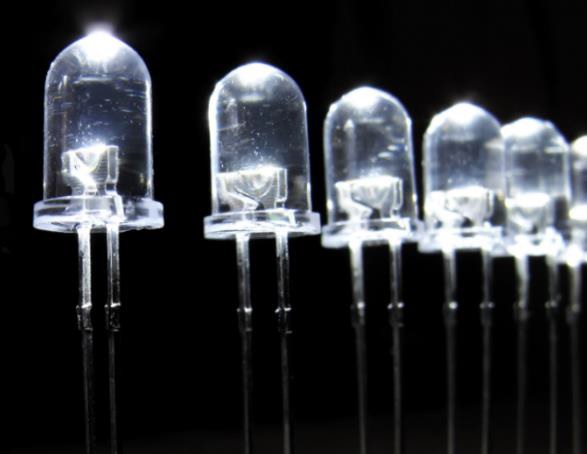
Picosun increases efficiency for LED and OLED production

News

Picosun Group has proved to significantly increase the production efficiency of its LED and OLED customers with the PICOSUN P-300BV ALD system. Recent tests show that a reduced ALD process cycle time and an increased number of wafers deposited with the same film thickness resulted in almost 100% better throughput. A throughput of over 20 000 wafers per month can be reached with a wafer batch of 100 wafers*. At the same time, the process quality in terms of film thickness uniformity has remained on an excellent level (<1% 1sigma) when measured within wafer, wafer to wafer as well as batch to batch.
“Picosun ALD solutions have become the standard in high volume ALD manufacturing. PICOSUN P-300BV ALD system is designed especially for production of LEDs and OLEDs. With our experience and deep know-how in ALD we are continuously striving to minimize the total cost of ownership and ensure future-proofness for our customers”, states Juhana Kostamo, Vice President, Industrial Business Area of Picosun Group.
Global LED and OLED manufacturers trust in ALD in their production to achieve better device performance and longer product lifetimes. This is a result of thin, conformal, uniform and pinhole-free material layers deposited by ALD for passivation and moisture protection as well as for creating buffer and interface layers.

* 4” 100 wafers, >20000 WPM, <1% 1sigma WiW, <1% 1sigma WtW, <1% 1sigma BtB (120 nm TMA + H2O @ 200 oC)


Purdue, imec, Indiana announce partnership
Resilinc partners with SEMI on supply chain resilience
NIO and NXP collaborate on 4D imaging radar deployment
Panasonic Industry digitally transforms with Blue Yonder
Global semiconductor sales decrease 8.7%
MIT engineers “grow” atomically thin transistors on top of computer chips
Keysight joins TSMC Open Innovation Platform 3DFabric Alliance
Leti Innovation Days to explore microelectronics’ transformational role
Quantum expansion
indie launches 'breakthrough' 120 GHz radar transceiver
Wafer fab equipment - facing uncertain times?
Renesas expands focus on India
Neuralink selects Takano Wafer Particle Measurement System
Micron reveals committee members
Avoiding unscheduled downtime in with Preventive Vacuum Service
NFC chip market size to surpass US$ 7.6 billion
Fujifilm breaks ground on new €30 million European expansion
Fraunhofer IIS/EAS selects Achronix embedded FPGAs
Siemens announces certifications for TSMC’s latest processes
EU Chips Act triggers further €7.4bn investment
ASE recognised for excellence by Texas Instruments
Atomera signs license agreement with STMicroelectronics
Gartner forecasts worldwide semiconductor revenue to decline 11% in 2023
CHIPS for America outlines vision for the National Semiconductor Technology Center
TSMC showcases new technology developments
Alphawave Semi showcases 3nm connectivity solutions
Greene Tweed to open new facility in Korea
Infineon enables next-generation automotive E/E architectures
Global AFM market to reach $861.5 million
Cepton expands proprietary chipset
Semtech adds two industry veterans to board of directors
Specialty gas expansion
×
Search the news archive

To close this popup you can press escape or click the close icon.
Logo
×
Logo
×
Register - Step 1

You may choose to subscribe to the Silicon Semiconductor Magazine, the Silicon Semiconductor Newsletter, or both. You may also request additional information if required, before submitting your application.


Please subscribe me to:


You chose the industry type of "Other"

Please enter the industry that you work in: