+44 (0)24 7671 8970
More publications     •     Advertise with us     •     Contact us
 
News Article

Picosun’s PicoArmour reduces semiconductor manufacturing costs

News

Picosun Group has pending patent rights for an ALD enabled corrosion protection solution against plasma etch that will bring benefits in semiconductor fabrication processes in terms of throughput, film uniformity and conformality. With PicoArmour the corrosion protection can be achieved more efficiently compared with the industry solutions commonly used today.
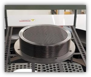
Wafer fabrication process flows include several steps where plasma etching is necessary. An inevitable consequence of using etching chemicals is that the tool itself will be etched. A common industrial solution for reducing the tool damage is applying a corrosion-resistant coating to the etch tool using for example PVD or spray coating with Y2O3. Compared to only using Y2O3, PicoArmour enables an up to five times faster and a more cost-effective way of producing the coating. Compared to Al2O3, the coating can be five times more durable.* Also, the maintenance interval of etch tools can be increased which also translates to significant reduction of manufacturing costs.
“Picosun’s approach with PicoArmour is to combine the highly-etch-resistant Y2O3 ALD process with more robust ALD processes. A high performance ALD corrosion barrier combining the speed and convenience of Al2O3 process with the durability of Y2O3 can be achieved by carefully controlling the film composition. With ALD, the protective effect can be achieved with thinner films, which in turn leads to material savings and a more environmentally friendly process”, states Juhana Kostamo, VP, Industrial Business Area of Picosun Group.

Purdue, imec, Indiana announce partnership
Resilinc partners with SEMI on supply chain resilience
NIO and NXP collaborate on 4D imaging radar deployment
Panasonic Industry digitally transforms with Blue Yonder
Global semiconductor sales decrease 8.7%
MIT engineers “grow” atomically thin transistors on top of computer chips
Keysight joins TSMC Open Innovation Platform 3DFabric Alliance
Leti Innovation Days to explore microelectronics’ transformational role
Quantum expansion
indie launches 'breakthrough' 120 GHz radar transceiver
Wafer fab equipment - facing uncertain times?
Renesas expands focus on India
Neuralink selects Takano Wafer Particle Measurement System
Micron reveals committee members
Avoiding unscheduled downtime in with Preventive Vacuum Service
NFC chip market size to surpass US$ 7.6 billion
Fujifilm breaks ground on new €30 million European expansion
Fraunhofer IIS/EAS selects Achronix embedded FPGAs
Siemens announces certifications for TSMC’s latest processes
EU Chips Act triggers further €7.4bn investment
ASE recognised for excellence by Texas Instruments
Atomera signs license agreement with STMicroelectronics
Gartner forecasts worldwide semiconductor revenue to decline 11% in 2023
CHIPS for America outlines vision for the National Semiconductor Technology Center
TSMC showcases new technology developments
Alphawave Semi showcases 3nm connectivity solutions
Greene Tweed to open new facility in Korea
Infineon enables next-generation automotive E/E architectures
Global AFM market to reach $861.5 million
Cepton expands proprietary chipset
Semtech adds two industry veterans to board of directors
Specialty gas expansion
×
Search the news archive

To close this popup you can press escape or click the close icon.
Logo
×
Logo
×
Register - Step 1

You may choose to subscribe to the Silicon Semiconductor Magazine, the Silicon Semiconductor Newsletter, or both. You may also request additional information if required, before submitting your application.


Please subscribe me to:


You chose the industry type of "Other"

Please enter the industry that you work in: