

Acoustically imaging the most elusive defects
Most defects are easily found before assembly by ultrasound in the form
of an Acoustic Micro Imaging (AMI) tool, which fires ultrasound pulses
into a component and analyzes the return echoes to identify defects, but
some remain elusive.
BY TOM ADAMS, CONSULTANT, NORDSON SONOSCAN
CRACKS, delaminations, non-bonds and voids are among the names used for internal gap-type structural defects that may occur in electronic packages. They may, in service, react to thermal and mechanical forces in a manner that breaks electrical connections.
Most such defects are easily found before assembly by ultrasound in the form of an Acoustic Micro Imaging (AMI) tool, which fires ultrasound pulses into a component and analyzes the return echoes to identify defects. Components having defects are removed from production.
As the tool’s scanning transducer moves along above an electronic component, it fires tens of thousands of pulses per second into the component. Each pulse is launched at a specific x-y location, and will send back echoes from internal material interfaces, such as mold compound to silicon, that it encounters. The echoes are rich in information, and each one determines the color or grey shade of a pixel in
the acoustic image.
The component being scanned may contain two types of internal interfaces:
Bonded interfaces between two solids such as mold compound and silicon. Solid-to-solid interfaces reflect part of the pulse and transmit the rest deeper into the component.
Interfaces between a solid and air. The air may have been incorporated into the device during fabrication. Solid-to-air interfaces reflect virtually all of the ultrasound back to the transducer. None travels into or through the air.
The solid-to-air interfaces are the top surfaces of voids, cracks and other internal structural defects containing air. Thermal or mechanical stresses may cause such a gap to expand and break electrical connections within the component. There are also internal anomalies that do not contain air. They are solid features that may be tilted, warped, or in the wrong place.
Most air-gap defects are easily detected and imaged by the AMI tool. The scanning transducer sends out tens of thousands of pulses per second as it scans at high speed over the component’s surface. Each pulse is aimed at a specific x-y location on the component’s surface and travels into the component. The transducer collects the echoes from internal interfaces from one location before it arrives at the next x-y location and launches the next pulse. In many of the imaging modes developed for the Nordson SONOSCAN C-SAM® tools, the highest-amplitude (“loudest”) return echo at a given x-y location determines the color of the pixel at that location. 
Figure 1. Echo reflection (1) from solid-to-solid interfaces, and (2) from a solid-to-air interface.
If a high-resolution 230 MHz transducer is being used, it is actually firing pulses with frequency content ranging from about 160 MHz to about 300 MHz. An outgoing pulse contains all of the frequencies in this range. The return echo can be differently distributed among the various frequencies depending on the nature of the interface. Typically, when the return echo arrives at the transducer, its amplitude is used to determine the pixel color for that x-y location. This is the sequence in what is called the Time Domain mode, in which other aspects of the echo (frequency, arrival time, polarity) are ignored.
The pulse-echo sequence is demonstrated in detail in Figure 1. The length and width of the arrow representing each pulse or echo approximates its amplitude.
At left in Frame 1, the scanning transducer has fired a pulse into the top of a component. It travels through the first layer of material and strikes the interface between the first and second material layers. A portion of its energy is reflected upward toward the transducer.
In Frame 2, the remainder of the pulse encounters no anomalies. At the interface it crosses into the third layer, while a portion of its energy is again sent back to the transducer.
In Frame 3, the now much smaller pulse stakes the interface, and an even smaller echo is returned to the transducer.
In the right half of the diagram -in Frame 1, the events are essentially the same as in the left half.
But the portion of the pulse that enters Frame 2 finds not a solid-to-solid interface, but the top surface of a void - in other words, a solid-to-air interface. Essentially all of the pulse’s energy is returned to the transducer as a high-energy echo. Note that the size of the reflected echo is the same as that of the arriving pulse. No energy remains to enter the third material. At the x-y location of the echo, no interfaces directly below this point will be imaged.
But in some cases, an air-filled defect remains invisible to ultrasound. How does this happen?
As noted earlier, a 230 MHz pulse contains all frequencies from about 160 MHz to about 300 MHz. The frequency content in an echo created by this pulse will cover the same range, but possibly with a different distribution of frequencies.
But some solid-to-air interfaces may not be microscopically smooth, meaning that they can scatter the reflected ultrasound in various directions. The echo that returns to the transducer may have a unique frequency distribution. Air-gap defects of this type many be invisible to standard Time Domain imaging.
Each pulse striking the solid-to-air interface sends back an echo that includes all of the frequencies in the pulse, but a short range within those frequencies can be reflected at higher amplitude. In most modes, such as Time Domain imaging, the transducer selects the highest amplitude among all the echoes arriving at an x-y location to assign a color for each x-y location. In this situation it is possible for the smaller echoes and frequency-sensitive reflections to escape detection.

Figure 2. Acoustically bright defect at right was not found by standard imaging.
Figure 2 shows a small area of a large chip suspected of having a defect that had escaped detection by Time Domain imaging. At left is the standard high-resolution 230 MHz Time Domain image, which shows no bright white areas that would indicate air gaps. Time Domain is an imaging mode that makes images based on the amplitude of the echo arriving from each of thousands of x-y locations within a specified time gate. The system typically selects the highest amplitude echo arriving at a given x- y location to determine the pixel color.
The image at left shows no bright areas that would indicate air gaps. Intent on finding a defect if one was present, researchers decided to use another resource: the Virtual Rescanning Module, or VRM. This mode first scans the component and in the process acquires the echo’s amplitude. frequency and travel time from the interface to the component’s surface.
VRM produces a matrix file containing all of the echoes from the entire volume of the component. The user can employ the matrix file to rapidly generate one image of the component at any of the frequencies between 160 and 300 MHz. Scanning of this ‘slide show’ can be done with either Time Domain or Frequency Domain imaging. At some point the user may find an image with a feature or features that did not show up in Time Domain imaging. In Figure 2, the frequency range in which the bright white defect appeared is in the range from 195 to 201 MHz.
The Frequency Domain scanned the VRM echoes of the area that had originally been scanned by the Time Domain. Scanning produced a single-frequency image of the area at each frequency generated by the 230 MHz transducer - that is, from 160 MHz to 300 MHz. Of these numerous images, only those in the 195-201 MHz range revealed the air gap near the right edge as a bright feature, seen in the right side of Figure 2.
All the other frequencies lacked the image of the air gap and looked much like the Time Domain image at left. Conclusion: the bright white feature in the Frequency Domain image is an air gap and could easily have caused an electrical failure. But the air gap could only be revealed by going beyond the imaging modes customarily used for high-volume screening.

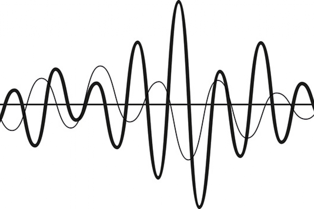
Figure 3. A defect may alter the range of frequency content of an echo.
Figure 3 shows what can happen at the solid-to-air interface to cause the air gap to become harder to detect with Time Domain imaging. In the top diagram, the incoming pulse from the transducer shows the orderly distribution of the wide range of frequencies as they are traveling through the component, and before they strike a material interface that will reflect them. If the interface has no irregularities, the return echo will have the same distribution of ultrasonic frequencies as the pulse. But if an interface is not smooth, or if the air gap is not clean and unbroken, the distribution of frequencies changes, as seen in the hypothetical lower diagram in Figure 3.
The V-shaped irregularity in the bottom diagram marks the distribution of the 195-201 MHz reflection from each x-y location at the solid-to-air interface. Each echo from this interface will produce a bright white pixel, while locations outside the defect will produce darker pixels. The user is now free to use the Frequency Mode as part of high-throughput screening to mark for rejection any component in which this defect occurs.


