Scaling 3D chips with molybdenum-based metallisation
Kaihan Ashtiani, Corporate Vice President and is General Manager of ALD/CVD Metals Product Group at Lam Research, discusses the reasons behind the chip industry’s new focus on Molybdenum, explains why this metal is critical to the future of computing, the three main challenges when it comes to current Atomic Deposition Layer (ALD) methods and how the company has stepped in to develop the ALTUS Halo molybdenum deposition tool, which overcomes these obstacles and helps to underpin the metal’s benefits in the era of smaller, faster and more sophisticated 3D chips
Advancing semiconductor materials and processes for the AI era
The digital world is transforming at an unprecedented pace, with artificial intelligence (AI) leading a wave of data-intensive applications that demand increasingly powerful computing platforms. At the heart of this transformation lies the semiconductor industry, which is undergoing its own revolution to meet the growing computational and memory requirements of modern digital technologies. AI and other data-centric applications are creating pressures on semiconductors to be smaller, faster, and more sophisticated, requiring advances not only in chip design but also in materials science and process technologies.
The evolution of semiconductor technology is a one-way journey, driven by the pervasive role that computers, smartphones, and other digital devices now play in everyday life. The performance requirements of these devices are accelerating rapidly, creating a continuous demand for innovations that push the limits of current semiconductor capabilities. The industry’s response to these demands is multifaceted, spanning improvements in computational capacity, memory performance, and interconnect efficiency, all of which are essential for realizing the next generation of digital devices. As a result, semiconductor companies are investing heavily in both materials innovation and high-precision manufacturing equipment, enabling the production of chips that operate faster, more efficiently, and at greater scale than ever before.
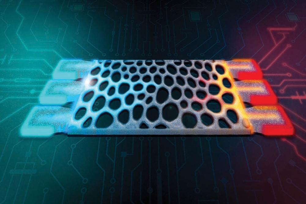
One area where these technological pressures are particularly visible is in the realm of metalization, a critical process in chip fabrication. Traditional metals such as copper and tungsten have long been the materials of choice for interconnects, the pathways that carry electrical signals across semiconductor devices. However, the shift toward 2.5D and 3D chip architectures, with multiple layers and increasingly complex electrical connectivity, is exposing the limitations of these conventional materials. The industry now faces a critical inflection point where new metals with superior properties must be employed to maintain performance as device dimensions continue to shrink.
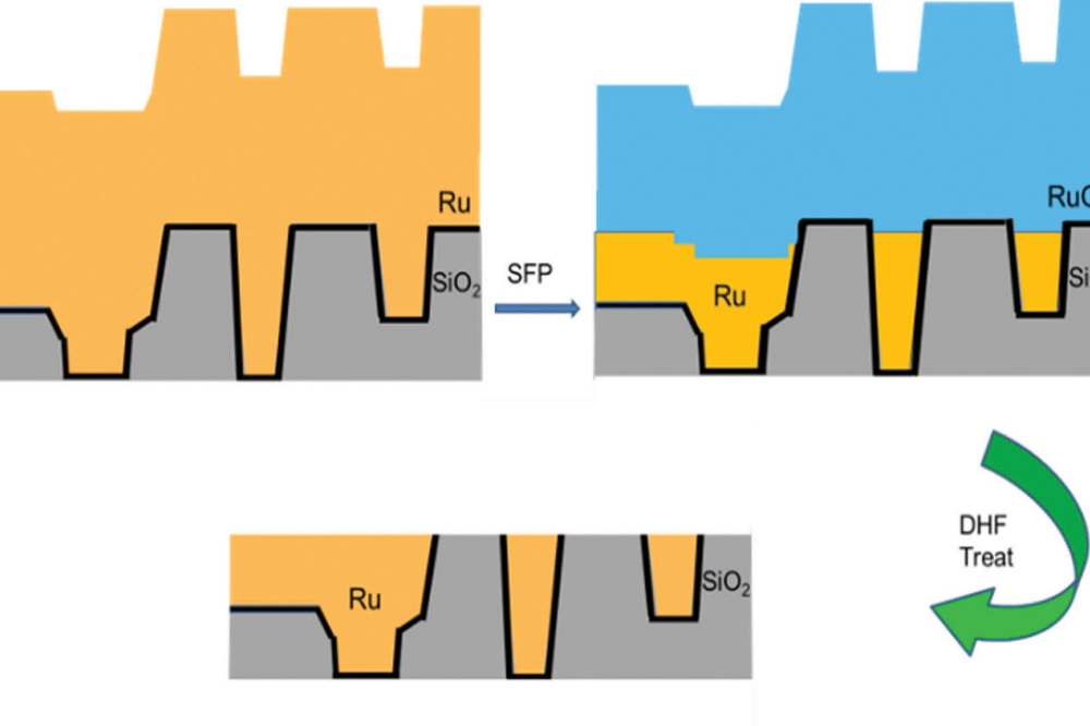
The challenge arises from a phenomenon known as thin-film resistivity. While the bulk resistivity of metals like copper and tungsten is well understood, their behaviour in extremely thin films - on the order of nanometers - introduces additional complexity. As the thickness of an interconnect approaches or falls below the mean free path of electrons within the material, the resistivity increases due to electron scattering. This effect becomes particularly significant at the transistor level and in the first few layers of interconnects, where high-speed signal transfer is essential. The combination of bulk resistivity and mean free path forms a figure of merit that dictates the suitability of a given metal for these ultra-thin applications. When copper and tungsten reach the limits of their performance under these conditions, the search for alternative metals becomes necessary.
Molybdenum has emerged as a promising candidate for these high-performance interconnects. Among the many elements in the periodic table, molybdenum offers a combination of electrical conductivity, thermal stability, and process compatibility that makes it ideal for replacing tungsten in critical areas of advanced semiconductor devices. The transition to molybdenum is not a wholesale replacement; it is targeted to specific layers where thin-film resistivity poses a limitation. By integrating molybdenum interconnects at these critical points, chip manufacturers can maintain high signal integrity and improve overall device performance, particularly in memory and logic applications where scaling continues unabated.

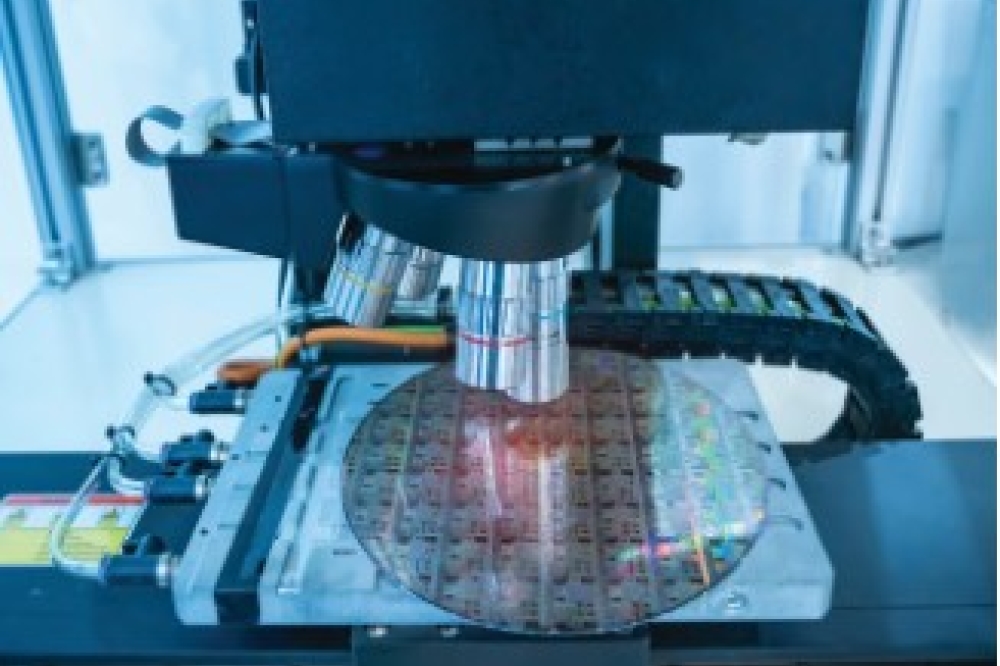
Achieving this transition, however, requires more than just identifying the right material. The deposition of molybdenum must be executed with extraordinary precision, which is where atomic layer deposition (ALD) technology becomes essential. ALD enables the controlled deposition of materials one atomic layer at a time, and in some cases even half a layer, ensuring that the properties of the deposited metal meet the stringent requirements for modern semiconductor devices. As chip dimensions shrink to scales thousands of times smaller than a human hair, precision deposition becomes critical not only for performance but also for yield and uniformity across large wafer surfaces.
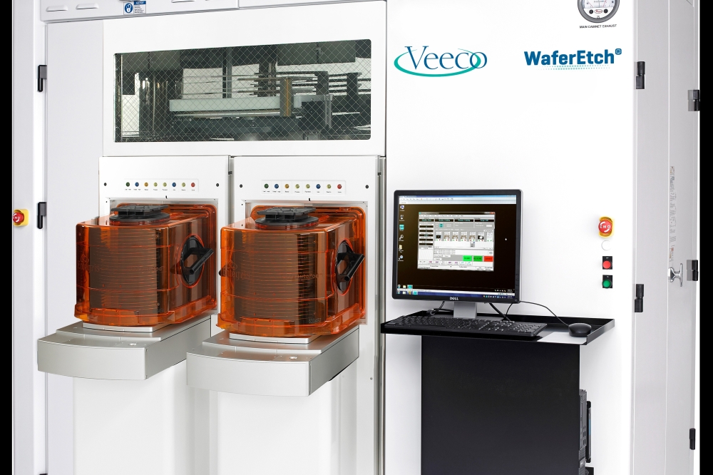
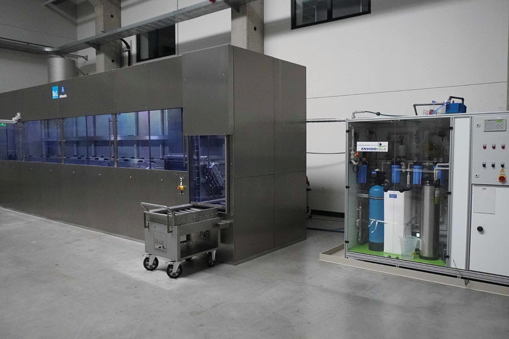
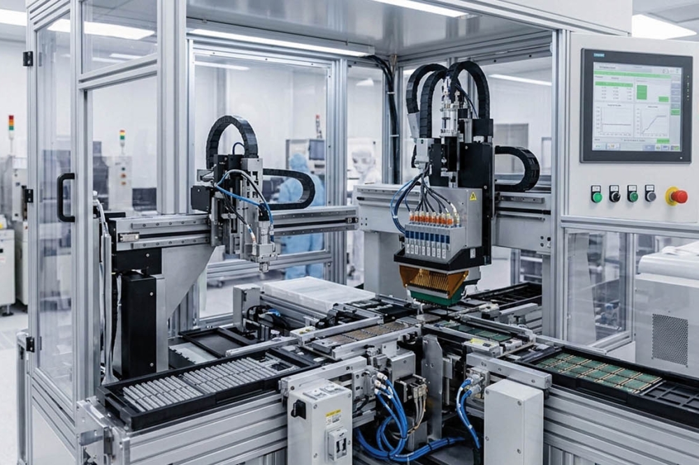
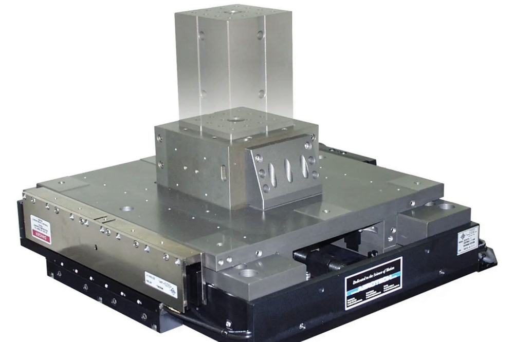
Lam Research’s recent introduction of the ALTUS Halo ALD tool exemplifies the level of innovation required to meet these challenges. Building on two decades of experience in ALD, including pioneering the first high-volume manufacturing of tungsten ALD, Lam has developed a tool capable of handling the unique challenges presented by molybdenum. Unlike tungsten, which can be delivered as a liquid precursor with high vapor pressure, molybdenum is deposited from a solid precursor. This necessitates careful sublimation, gas transport, and precise thermal management to deliver the material uniformly to the wafer. The ALTUS Halo system integrates proprietary hardware and process sequences to ensure that each atomic layer of molybdenum maintains the desired electrical properties, enabling faster, more efficient chip performance.
Developing the ALTUS Halo was not simply a matter of adapting existing techniques. The project involved extensive collaboration with chemical vendors to create a suitable molybdenum precursor and delivery system. Lam’s expertise in ALD processes, built over decades, was applied to design a system capable of delivering solid precursors reliably in a high-volume manufacturing environment. This required sophisticated engineering to control temperature, gas flow, and deposition sequences, ensuring that every wafer processed meets the stringent electrical and structural requirements of advanced semiconductor devices. The integration of hardware precision and process expertise allowed LAM to overcome the unique challenges posed by molybdenum and introduce a tool that has been well received across the semiconductor industry.
The successful deployment of the ALTUS Halo highlights the importance of collaboration across the semiconductor supply chain. High-volume manufacturing of advanced devices relies on a close partnership between equipment suppliers, chemical vendors, and chip manufacturers. Each stakeholder contributes critical expertise, from precursor chemistry to process integration and device validation. For memory applications, including DRAM and NAND flash, as well as logic and foundry processes, the precise integration of molybdenum interconnects requires iterative evaluation of electrical performance and process compatibility. Only through this comprehensive collaboration can a new material and deposition tool be qualified for high-volume semiconductor production, where reliability and reproducibility are paramount.
The introduction of molybdenum via ALD is not the endpoint but rather a foundation for continuous improvement. The pace of innovation in semiconductors is relentless, driven by the need to support increasingly powerful AI applications and the broader digital ecosystem. Once a material and process are deployed in manufacturing, the work does not stop. Continuous improvement plans, known in the industry as CIPs, are implemented to optimize tool productivity, enhance material properties, and anticipate the requirements of next-generation devices. Even as molybdenum ALD becomes a long-lasting technology, ongoing refinements are necessary to address increasingly stringent performance and cost requirements. This iterative development ensures that the technology remains viable and competitive for the next five to ten years and beyond.
The role of materials innovation extends beyond electrical performance. Selecting the appropriate material involves considering factors such as thermal conductivity, mechanical stability, and compatibility with other process steps. In the case of molybdenum, its unique combination of properties makes it suitable for integration into multilayer interconnect structures, facilitating the continued miniaturization of semiconductor devices. The ability to deposit this material with atomic precision is critical to leveraging its advantages fully, and it underscores the broader importance of materials research in driving the semiconductor industry forward.
From a broader perspective, the adoption of molybdenum ALD reflects a paradigm shift in semiconductor manufacturing. As device dimensions shrink and computational demands grow, traditional materials and processes can no longer meet the performance targets required for modern applications. The transition to new metals, coupled with high-precision deposition techniques, represents a fundamental advancement in the industry’s capability to deliver faster, more efficient, and more reliable semiconductor devices. This innovation is particularly critical for AI workloads, which require massive computational throughput, low latency, and high memory bandwidth, all of which depend on optimized interconnect performance.
The impact of these advancements extends across the digital ecosystem. Faster interconnects enable higher data transfer rates within chips, improving the performance of everything from consumer electronics to large-scale server farms that power cloud computing and AI inference. Memory chips benefit from reduced resistivity and improved signal integrity, enabling higher-density storage and faster access times. Logic devices gain enhanced performance through lower latency interconnects, supporting more complex computation and accelerating AI model training and deployment. Collectively, these improvements contribute to a broader trend of digital acceleration, where semiconductors continue to drive innovation in virtually every sector of technology.
Lam Research’s ALTUS Halo ALD tool exemplifies the synthesis of materials science, process engineering, and supply chain collaboration. By overcoming the challenges of depositing molybdenum with atomic precision, the tool demonstrates how equipment innovation can unlock new material capabilities, directly impacting the performance of semiconductor devices. This achievement underscores the broader principle that semiconductor advancement is not solely about device design but also about enabling technologies that make new materials practical and reliable at scale.
Looking ahead, the development of tools like the ALTUS Halo points to a future in which semiconductor innovation continues to accelerate. While molybdenum ALD represents a significant milestone, ongoing research and development will be required to address the next generation of device architectures, further miniaturization, and emerging applications in AI, high-speed networking, and beyond. Continuous improvement initiatives ensure that even established technologies evolve to meet higher performance standards, greater throughput demands, and tighter cost constraints. In this way, the semiconductor industry remains in a constant state of technological evolution, responding to the ever-expanding demands of the digital world.
The journey from material discovery to high-volume manufacturing is complex, involving multiple layers of collaboration, innovation, and engineering. Identifying an element with desirable electrical properties is only the first step; translating that discovery into a scalable, reliable process requires sophisticated equipment, precise control, and rigorous validation. Lam’s experience with ALD over the past two decades highlights how expertise in both hardware and process development is essential for introducing new materials into semiconductor production. The integration of molybdenum into advanced interconnect structures demonstrates the practical application of these principles, providing a blueprint for future innovations in semiconductor materials and processes.
In conclusion, the semiconductor industry is at a pivotal moment, driven by the dual forces of increasing computational demand and device miniaturization. AI and other digital applications are accelerating the need for advanced materials and precise manufacturing techniques, challenging the industry to innovate at every level. The adoption of molybdenum interconnects via atomic layer deposition exemplifies how materials science, process engineering, and collaborative development converge to meet these challenges. Tools like the ALTUS Halo not only enable the production of faster and more efficient semiconductor devices but also provide a platform for continuous improvement and future innovation. As the digital world continues to evolve, the ability to translate fundamental materials discoveries into practical, scalable manufacturing solutions will remain a defining feature of semiconductor technology, ensuring that the industry can support the next generation of computational demands and maintain its central role in driving technological progress. The relentless pace of innovation ensures that semiconductor companies, researchers, and engineers remain at the forefront of technological advancement, constantly pushing the boundaries of what is possible.