+44 (0)24 7671 8970
More publications     •     Advertise with us     •     Contact us
 
News Article

ST chip sets miniaturisation record for mobile functionality

News


STMicroelectronics has introduced what it claims is the world's smallest TVS diode for protecting sensitive electronics in consumer products and handhelds.

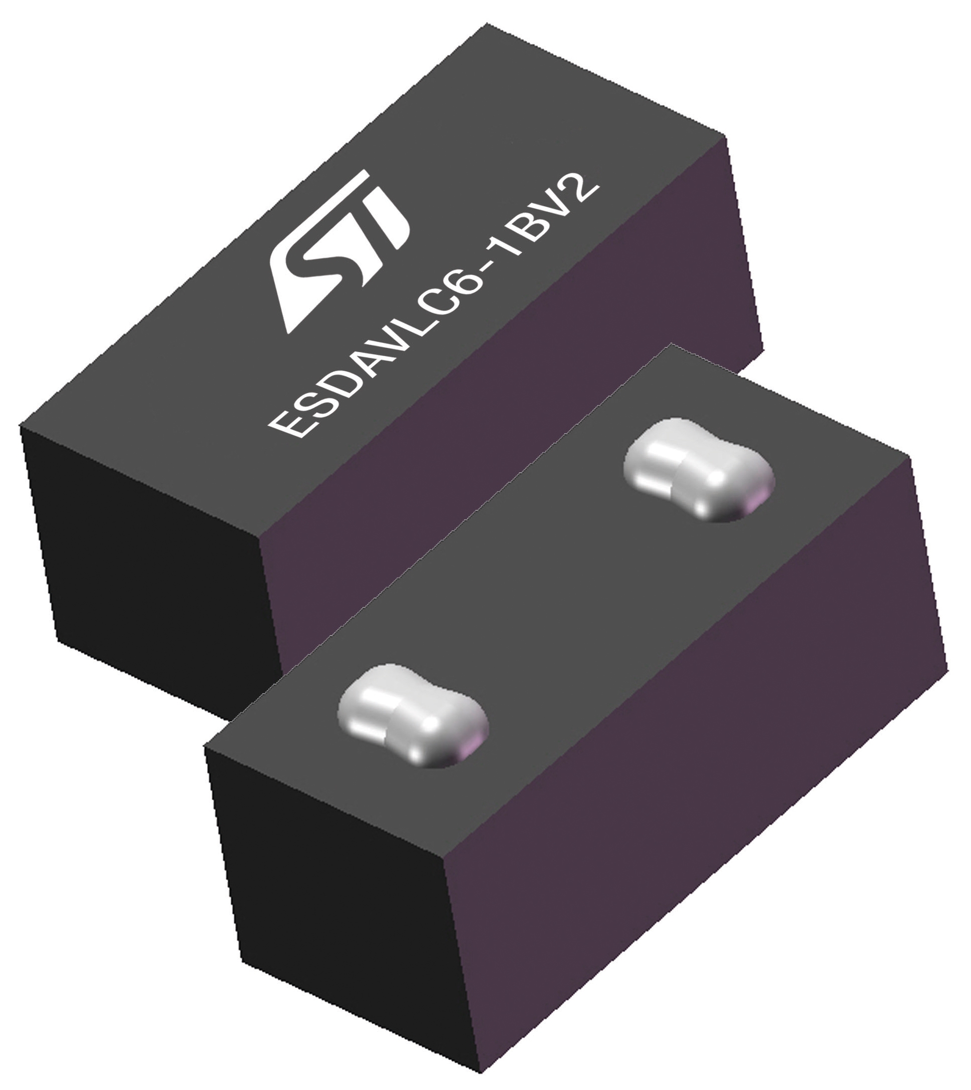
As the first such device to be offered in the industry's smallest standard surface-mount outline of 0.45 x 0.2mm, the ESDAVLC6-1BV2 is one size smaller than today's 0.6 x 0.3mm devices.

The value of the space saving to designers can be seen by comparing with other chip sizes used in smartphones and tablets.

"A complete motion-sensing IC for features such as indoor navigation and advanced user interface, such as ST's LSM303D, measures just 3 x 3mm, while some power chips are as small as 2 x 2mm," explains Eric Paris, Product Marketing Director, ASD & IPAD Division, STMicroelectronics.

"Trimming 0.2mm or 0.1mm from each TVS can simplify placing components and routing connections, especially if the design contains several such devices."

The ESDAVLC6-1BV2 TVS diode fully satisfies the protection requirements specified in the international standard IEC 61000-4-2. Although other types of electrostatic-discharge (ESD) protectors, such as varistors, are available in the same size, these generally do not protect as effectively.

ST's new ESDAVLC6-1BV2 has a clamping voltage half that of the nearest competing varistor in the same size package, offering greater safety for the internal components. Although useful in many applications, varistors also age, providing progressively less protection with each ESD event clamped.

The ESDAVLC6-1BV2 is in mass production now, and samples are also available. Prices start at $0.10 for orders of 1,000 pieces.


Purdue, imec, Indiana announce partnership
Resilinc partners with SEMI on supply chain resilience
NIO and NXP collaborate on 4D imaging radar deployment
Panasonic Industry digitally transforms with Blue Yonder
Global semiconductor sales decrease 8.7%
MIT engineers “grow” atomically thin transistors on top of computer chips
Keysight joins TSMC Open Innovation Platform 3DFabric Alliance
Leti Innovation Days to explore microelectronics’ transformational role
Quantum expansion
indie launches 'breakthrough' 120 GHz radar transceiver
Wafer fab equipment - facing uncertain times?
Renesas expands focus on India
Neuralink selects Takano Wafer Particle Measurement System
Micron reveals committee members
Avoiding unscheduled downtime in with Preventive Vacuum Service
NFC chip market size to surpass US$ 7.6 billion
Fujifilm breaks ground on new €30 million European expansion
Fraunhofer IIS/EAS selects Achronix embedded FPGAs
Siemens announces certifications for TSMC’s latest processes
EU Chips Act triggers further €7.4bn investment
ASE recognised for excellence by Texas Instruments
Atomera signs license agreement with STMicroelectronics
Gartner forecasts worldwide semiconductor revenue to decline 11% in 2023
CHIPS for America outlines vision for the National Semiconductor Technology Center
TSMC showcases new technology developments
Alphawave Semi showcases 3nm connectivity solutions
Greene Tweed to open new facility in Korea
Infineon enables next-generation automotive E/E architectures
Global AFM market to reach $861.5 million
Cepton expands proprietary chipset
Semtech adds two industry veterans to board of directors
Specialty gas expansion
×
Search the news archive

To close this popup you can press escape or click the close icon.
Logo
×
Logo
×
Register - Step 1

You may choose to subscribe to the Silicon Semiconductor Magazine, the Silicon Semiconductor Newsletter, or both. You may also request additional information if required, before submitting your application.


Please subscribe me to:


You chose the industry type of "Other"

Please enter the industry that you work in: