
Burgeoning glass wafer market to hit 1.3 billion by 2018
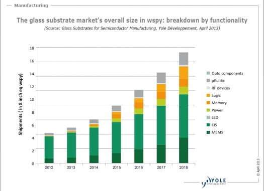
MEMS and CMOS image sensors currently dominate the market, but Memory, Logic ICs and LEDs will start to increase market share in the future
Glass is everywhere: from MEMS, CMOS image sensors and power to memory, logic IC and microfluidics.
Glass is widely used in everyday life and found in large quantities in many industries, such as flat panel display applications. Over the last few years, glass has gained considerable interest from the semiconductor industry due to its very attractive electrical, physical and chemical properties, as well as its prospects for a relevant and cost-efficient solution.
The application scope of glass substrates in the semiconductor field is broad and highly diverse.
End-applications include MEMS, CMOS Image Sensors, LED, Memory, Logic IC, RF/Analogue ICs, Power, micro-batteries, Optoelectronic components and Microfluidics
Glass wafers can be used as a support substrate, for WLCapping, as 3D TGV/2.5D interposers, carriers and in micro-structuring.
The demand for glass is growing, and glass has already been adapted for various and unique wafer-processing functionalities and platforms supporting a wide range of end-applications. For example, WLCapping is driven mainly by MEMS and CMOS Image Sensors.
In the coming years, the availability of other glass functionalities such as 3D TGV/2.5 D interposers in conjunction with end-applications like Memory and Logic ICs will be the driving force for growth, creating new challenges and new technical developments along the way.
Yole Développement's "Glass Substrates for Semiconductor Manufacturing" report says the market is mainly driven by the Wafer-Level Packaging industry. The glass wafer market is expected to grow from $158 million in 2012 to a massive $1.3 billion by 2018, at a CAGR of about 41 percent over the next five years.
"Initially driven by CMOS Image Sensor and MEMS applications, this growing industry will be supported by relevant end-applications such as LED, memory and logic IC, where glass is on its way to being commercialised. In terms of wafers shipped, a 4 x glass wafer growth is expected in the semiconductor industry over the next five years, achieving more than 15 million 8" EQ WSPY by 2018," explains Amandine Pizzagalli, Market and Technology Analyst, Equipment & Materials Manufacturing, at Yole Développement.
The glass WLCapping platform is a mature functionality already adopted with significant volume in CMOS Image Sensors, where more than 3.3 million glass caps were shipped in 2012. This market is expected to grow slowly, with a CAGR of 14 percent from 2012 to 2018, mainly supported by MEMS devices impacted by the request for further miniaturisation. On the flip side, the glass market for WLOptics is likely to decline from 2015 to 2018 due to the development of competing technologies.
All of this said, Yole expects to see strong growth in the glass market, mainly supported by two emerging WLP platforms: with a CAGR of 110 percent and 70 percent respectively, the glass-type 2.5D interposer emerging platform and the carrier wafer will be glass' fastest-growing fields over the next five years, since glass offers the best value proposition in terms of cost, flexibility, mechanical rigidity and surface flatness.
If glass is qualified for 2.5D interposer functionality, the glass market could exceed $1 billion revenue by 2018. However, it's still unclear how BEOL wafer fabs will choose glass over the current silicon technology used for logic IC applications (for the 2.5D/3D SOC and system partitioning areas), but the glass variety of 2.5D interposer substrates is expected to significantly impact future glass wafer demand, and it's obvious that the 2.5D Glass interposer will attract many newcomers.
The use of glass interposers in packaging will certainly be on the HVM roadmap within a few years.
The top five glass substrate players hold almost 80 percent of the market. In the semiconductor industry, the glass substrate market is split amongst five main suppliers. Schott (G), Tecnisco (JP), PlanOptik (G), Bullen (US) and Corning (US) will share more than 70 percent $158 million glass substrate market this year, driven mainly by demand for WLCapping.
In the midst of this growing market, semiconductor glass suppliers are trying to differentiate themselves by proposing a variety of glass substrate material properties with a good CTE, solid thermal properties and no polishing/grinding steps required, which would result in reduced costs.
Many glass substrate suppliers such as AGC, Corning and HOYA are expected to increase their business in the next few years since they are quite aggressive in 2.5D interposers and glass carrier wafers, and are expected to ramp-up into high volume production. Since the big players are already deeply entrenched in the glass market, it will be very challenging for a new entrant to break through in the foreseeable future.


