+44 (0)24 7671 8970
More publications     •     Advertise with us     •     Contact us
 
News Article

Camtek receives another order for TEM sample preparation tool

News


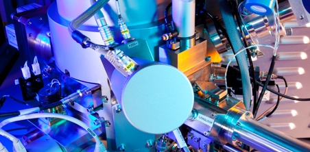
The Xact200 system pictured above is designed to make transmission electron microscopy (TEM) sample preparation easier

Camtek has received a repeat order for its next generation TEM sample preparation system.

The firm has received the order from the customer after a previous purchase of the tool over a year ago. 

Shrinking feature dimensions and advances in material complexity require a scale of analysis which are arguably only possible through Transmission Electron Microscope (TEM) processes. 

Xact200 performs cutting-edge TEM sample preparation in line with semiconductor and nanotechnology roadmap requirements, for physical failure analysis and characterization.

Roy Porat, Camtek' s Chief Executive Officer, comments, "Camtek penetrated the sample preparation market with the acquisition of SELA in 2010. This order represents a milestone after over a year in which we invested a lot of efforts in improving and maturing the product. I am pleased with the progress we have made with Xact200, and look forward to seeing additional installations in the coming months."

Camtek Ltd. provides automated and technologically advanced solutions dedicated to enhancing production processes and increasing yields, enabling and supporting customer's latest technologies in the semiconductors, printed circuit boards and IC substrates industries.

Camtek addresses the specific needs of these interconnected industries with dedicated solutions based on a wide and advanced platform of technologies including intelligent imaging, image processing, adaptive ion milling and digital material deposition.

The firm's solutions range from micro-to-nano by applying its technologies to the industries' specific requirements.

Purdue, imec, Indiana announce partnership
Resilinc partners with SEMI on supply chain resilience
NIO and NXP collaborate on 4D imaging radar deployment
Panasonic Industry digitally transforms with Blue Yonder
Global semiconductor sales decrease 8.7%
MIT engineers “grow” atomically thin transistors on top of computer chips
Keysight joins TSMC Open Innovation Platform 3DFabric Alliance
Leti Innovation Days to explore microelectronics’ transformational role
Quantum expansion
indie launches 'breakthrough' 120 GHz radar transceiver
Wafer fab equipment - facing uncertain times?
Renesas expands focus on India
Neuralink selects Takano Wafer Particle Measurement System
Micron reveals committee members
Avoiding unscheduled downtime in with Preventive Vacuum Service
NFC chip market size to surpass US$ 7.6 billion
Fujifilm breaks ground on new €30 million European expansion
Fraunhofer IIS/EAS selects Achronix embedded FPGAs
Siemens announces certifications for TSMC’s latest processes
EU Chips Act triggers further €7.4bn investment
ASE recognised for excellence by Texas Instruments
Atomera signs license agreement with STMicroelectronics
Gartner forecasts worldwide semiconductor revenue to decline 11% in 2023
CHIPS for America outlines vision for the National Semiconductor Technology Center
TSMC showcases new technology developments
Alphawave Semi showcases 3nm connectivity solutions
Greene Tweed to open new facility in Korea
Infineon enables next-generation automotive E/E architectures
Global AFM market to reach $861.5 million
Cepton expands proprietary chipset
Semtech adds two industry veterans to board of directors
Specialty gas expansion
×
Search the news archive

To close this popup you can press escape or click the close icon.
Logo
×
Logo
×
Register - Step 1

You may choose to subscribe to the Silicon Semiconductor Magazine, the Silicon Semiconductor Newsletter, or both. You may also request additional information if required, before submitting your application.


Please subscribe me to:


You chose the industry type of "Other"

Please enter the industry that you work in: