
News Article
Rudolph Launches Transparent Thin Film Metrology System
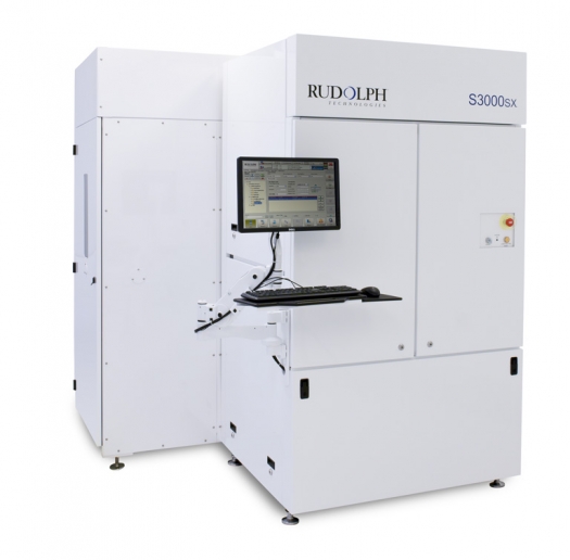
Rudolph Technologies, Inc, a supplier to the semiconductor, FPD, LED and solar industries, has announced the release of the S3000SX thin film metrology system for transparent films in advanced semiconductor fabrication applications at the 28nm node and below. This latest addition to the S3000 product family uses Rudolph's proprietary focused beam ellipsometry (FBE) and newly-designed small site measurement optics (SSMO) to measure the thickness of single layer and multi-layer films on product wafers including device area at sites sizes as small as 30x30 µm. Additionally, the S3000SX System continues Rudolph's flexible modular approach with a selection of new metrology capabilities that customers can tailor to their specific process requirements, optimizing the balance of performance and cost of ownership.
"Each node pushes the limits of semiconductor manufacturing processes and the control needed to maintain yield," said Dr. Mike Colgan, vice president and general manager of Rudolph's Metrology Business Unit. "Scaling to the 2x and 1x nodes continues to introduce novel materials, thinner multilayer film stacks, and the need for fast, accurate, on-product metrology. With its small site measurement capability and an array of unique metrology and productivity solutions, the S3000SX System offers the optimal combination of high performance and low cost of ownership for fab-wide metrology in logic, memory, foundry, and MEMS."
Rudolph's proprietary FBE uses three laser sources operating at different wavelengths to measure film thicknesses with industry-leading speed and precision without the need for complicated dispersion models. The laser's stability and accuracy permit easy matching between systems and its long lifetime minimizes downtime for maintenance. The S3000SX System adds a new shorter wavelength source (405 nm) and specialized small site measurement optics to permit single wavelength measurements in sites as small as 30X30 µm, and provides improved performance on SOI, thin films and SiGe. Available metrology options include deep UV (190 nm) reflectometry, wafer stress and bow measurements, and next-generation airborne molecular contaminant control.


