Fraunhofer & EVG bond to grow III-Vs on silicon

The aim of a joint project is to enable highly mismatched combinations such as GaAs-on-silicon
The Fraunhofer Institute for Solar Energy Systems ISE has joined forces with EV Group (EVG) to develop equipment and process technology to enable electrically conductive and optically transparent direct wafer bonds at room temperature.
The new solutions, developed in partnership with Fraunhofer ISE based on EVG's ComBond technology, aim to enable highly mismatched material combinations like gallium arsenide (GaAs) on silicon, GaAs on indium phosphide (InP), InP on germanium and GaAs on gallium antimonide (GaSb).
Direct wafer bonding provides the ability to combine a variety of materials with optimal properties for integration into multi-junction solar cells, which can lead to new device architectures with unparalleled performance.
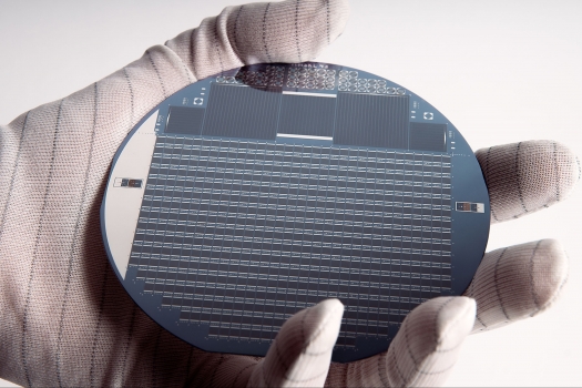
The image at the top of this story shows III-V multi-junction concentrator solar cells grown on a 4-inch diameter wafer. (Credit : Fraunhofer ISE).
"Using direct semiconductor bond technology developed in cooperation with EVG, we expect that the best material choices for multi-junction solar cell devices will become available and allow us to increase the conversion efficiency toward 50 percent," states Frank Dimroth, Head of department III-V - Epitaxy and Solar Cells of Fraunhofer ISE. "We are excited to partner with EVG, a leading supplier of wafer bonding equipment, to develop industrial tools and processes for this application."
Fraunhofer ISE has developed III-V multi-junction solar cells for more than 20 years and has reached record device efficiencies of up to 41 percent with its metamorphic triple-junction solar cell technology on germanium.
Higher efficiencies require the development of four- and five-junction solar cells with new material combinations to span the full absorption range of the sun's spectrum between 300-2000 nm.
Integration of III-V solar cells on silicon opens another opportunity to reduce manufacturing cost, especially when combined with modern substrate lift-off technologies.
Direct wafer-bonding is expected to play an important role in the development of next-generation III-V solar cell devices with applications in space as well as in terrestrial concentrator photovoltaics (PV).
"We are excited about refining our new process technology together with Fraunhofer ISE, the largest solar energy research institute in Europe," notes Markus Wimplinger, corporate technology development and IP director for EVG. "Fraunhofer ISE's broad expertise in the area of PV, specifically in concentrated PV cell manufacturing and photonics, will allow us to characterise bonding interfaces with respect to PV applications on our new ComBond equipment platform."
EVG's ComBond technology has been developed in response to market needs for more sophisticated integration processes for combining materials with different lattice constant and coefficient of thermal expansion (CTE).
The process and equipment technology enables the formation of bond interfaces between heterogeneous materials - such as silicon to compound semiconductors, compound semiconductors to compound semiconductors, germanium to silicon and germanium to compound semiconductors - at room temperature, while achieving excellent bonding strength.
The ComBond technology will be commercially available later this year on a new 200mm modular platform currently in development, called EVG580 ComBond, which will include process modules that are designed to perform surface preparation processes on both semiconductor materials and metals.
In addition to PV, other potential application areas for processes developed in cooperation between EVG and Fraunhofer ISE include silicon photonics and LEDs.


