+44 (0)24 7671 8970
More publications     •     Advertise with us     •     Contact us
 
News Article

Imec & Panasonic unveil 4K2K silicon CMOS image sensor

News

The co-developed imager sensor chip targets high speed, high resolution imaging applications such as next generation HDTV


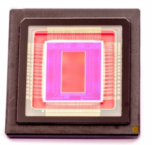
Imec is launching a CMOS image sensor capable of capturing 12-bit 4,000 x 2,000 pixel progressive images at 60 frames per second (fps).

Based on a stagger-laced dual exposure, the image sensor developed with Panasonic, was processed using imec's 130nm CMOS process on 200mm silicon wafers to deliver high-speed and high-quality imaging at a reduced output bit rate.

The number of pixels on image sensors in video and still cameras keeps increasing, along with the frame rate and bit resolution requirements of the images. 4K2K is expected to be the next-generation broadcasting format, offering an increase by a factor of two in both horizontal and vertical resolution compared to current state-of-the-art High Definition TV. 

The image sensor chip is a floating diffusion shared 4T pixel imager, with a pitch of 2.5 microns and a conversion gain of 70 μV/e-, which allows for both a classical rolling shutter or stagger-laced scanning mode.

The 4K2K 60-fps imaging performance is realised by 12-bit column-based delta-sigma A/D converters. The stagger-laced scanning method improves imaging sensitivity and provides a 50 percent reduction in output data rate by alternating the readout of two sets of horizontal pixel pairs arranged in two complementary checkerboard patterns. What's more, the overall power consumption of the imager is less than 2 W. 

"This is an important milestone for imec to demonstrate our capability to co-design, prototype and manufacture high performance CMOS image sensors in our 200 mm CMOS fab," says Rudi Cartuyvels, Senior Vice President Smart Systems & Energy Technologies at imec.

Purdue, imec, Indiana announce partnership
Resilinc partners with SEMI on supply chain resilience
NIO and NXP collaborate on 4D imaging radar deployment
Panasonic Industry digitally transforms with Blue Yonder
Global semiconductor sales decrease 8.7%
MIT engineers “grow” atomically thin transistors on top of computer chips
Keysight joins TSMC Open Innovation Platform 3DFabric Alliance
Leti Innovation Days to explore microelectronics’ transformational role
Quantum expansion
indie launches 'breakthrough' 120 GHz radar transceiver
Wafer fab equipment - facing uncertain times?
Renesas expands focus on India
Neuralink selects Takano Wafer Particle Measurement System
Micron reveals committee members
Avoiding unscheduled downtime in with Preventive Vacuum Service
NFC chip market size to surpass US$ 7.6 billion
Fujifilm breaks ground on new €30 million European expansion
Fraunhofer IIS/EAS selects Achronix embedded FPGAs
Siemens announces certifications for TSMC’s latest processes
EU Chips Act triggers further €7.4bn investment
ASE recognised for excellence by Texas Instruments
Atomera signs license agreement with STMicroelectronics
Gartner forecasts worldwide semiconductor revenue to decline 11% in 2023
CHIPS for America outlines vision for the National Semiconductor Technology Center
TSMC showcases new technology developments
Alphawave Semi showcases 3nm connectivity solutions
Greene Tweed to open new facility in Korea
Infineon enables next-generation automotive E/E architectures
Global AFM market to reach $861.5 million
Cepton expands proprietary chipset
Semtech adds two industry veterans to board of directors
Specialty gas expansion
×
Search the news archive

To close this popup you can press escape or click the close icon.
Logo
×
Logo
×
Register - Step 1

You may choose to subscribe to the Silicon Semiconductor Magazine, the Silicon Semiconductor Newsletter, or both. You may also request additional information if required, before submitting your application.


Please subscribe me to:


You chose the industry type of "Other"

Please enter the industry that you work in: