+44 (0)24 7671 8970
More publications     •     Advertise with us     •     Contact us
 
News Article

ZEISS launches photomask repair tool for EUV and HDMoSi

News

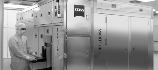
The new generation system MeRiT HR II from ZEISS offers a significantly higher degree of automation and increased flexibility in the repair of transparent and opaque defects.

Any defect geometry on all known as well as new mask types and materials can be processed: Binary, OMOG, HD MoSi and EUV. The technical specifications of the MeRiT HR II match to the industry roadmap and sharp market requirements.

The redesigned tool includes a sound automation package which enables a new level of automation with optimised repair flow. After a short setup routine the processes are able to seamlessly repair numerous defects without the need for human interaction.

A higher throughput due to lower idling time is also offered. In case of any doubt a security interlock consults the operator who can intervene when necessary.

"The significantly improved automation level of the new MeRiT HR II frees up precious operator time. Furthermore the combination of automation and manual repair provides an increased flexibility. Altogether the new system has its finger on the pulse as it includes the most relevant requirements mask shops have for repairing all kinds of photomask types in a very short time," says Oliver Kienzle, head of the ZEISS strategic business unit Semiconductor Metrology Systems who develops and sells the MeRiT HR II.

With improved repair processes the MeRiT HR II from ZEISS meets the repair specifications of today's and future repair nodes. The new generation tool MeRiT HR II will be presented at the ZEISS booth during the European Mask and Lithography Conference (EMLC) in Dresden, which takes part from June 25th to 27th, 2013.

Purdue, imec, Indiana announce partnership
Resilinc partners with SEMI on supply chain resilience
NIO and NXP collaborate on 4D imaging radar deployment
Panasonic Industry digitally transforms with Blue Yonder
Global semiconductor sales decrease 8.7%
MIT engineers “grow” atomically thin transistors on top of computer chips
Keysight joins TSMC Open Innovation Platform 3DFabric Alliance
Leti Innovation Days to explore microelectronics’ transformational role
Quantum expansion
indie launches 'breakthrough' 120 GHz radar transceiver
Wafer fab equipment - facing uncertain times?
Renesas expands focus on India
Neuralink selects Takano Wafer Particle Measurement System
Micron reveals committee members
Avoiding unscheduled downtime in with Preventive Vacuum Service
NFC chip market size to surpass US$ 7.6 billion
Fujifilm breaks ground on new €30 million European expansion
Fraunhofer IIS/EAS selects Achronix embedded FPGAs
Siemens announces certifications for TSMC’s latest processes
EU Chips Act triggers further €7.4bn investment
ASE recognised for excellence by Texas Instruments
Atomera signs license agreement with STMicroelectronics
Gartner forecasts worldwide semiconductor revenue to decline 11% in 2023
CHIPS for America outlines vision for the National Semiconductor Technology Center
TSMC showcases new technology developments
Alphawave Semi showcases 3nm connectivity solutions
Greene Tweed to open new facility in Korea
Infineon enables next-generation automotive E/E architectures
Global AFM market to reach $861.5 million
Cepton expands proprietary chipset
Semtech adds two industry veterans to board of directors
Specialty gas expansion
×
Search the news archive

To close this popup you can press escape or click the close icon.
Logo
×
Logo
×
Register - Step 1

You may choose to subscribe to the Silicon Semiconductor Magazine, the Silicon Semiconductor Newsletter, or both. You may also request additional information if required, before submitting your application.


Please subscribe me to:


You chose the industry type of "Other"

Please enter the industry that you work in: