
News Article
Transistors without silicon
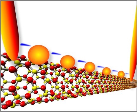
The room temperature tunnelling behaviour of boron nitride (BN) nanotubes has been demonstrated with the aid of gold quantum dots
For decades, electronic devices have been getting smaller, and smaller, and smaller. It’s now possible - even routine - to place millions of transistors on a single silicon chip.
But transistors based on semiconductors can only get so small.
“At the rate the current technology is progressing, in 10 or 20 years, they won’t be able to get any smaller,” notes physicist Yoke Khin Yap of Michigan Technological University. “Also, semiconductors have another disadvantage: they waste a lot of energy in the form of heat.”

Electrons flash across a series of gold quantum dots on boron nitride nanotubes. Michigan Tech scientists made the quantum-tunnelling device, which acts like a transistor at room temperature, without using semiconducting materials. (credit: Yoke Khin Yap)
Scientists have experimented with different materials and designs for transistors to address these issues, always using semiconductors like silicon. Back in 2007, Yap wanted to try something different that might open the door to a new age of electronics.
“The idea was to make a transistor using a nanoscale insulator with nanoscale metals on top,” he says. “In principle, you could get a piece of plastic and spread a handful of metal powders on top to make the devices, if you do it right. But we were trying to create it in nanoscale, so we chose a nanoscale insulator, boron nitride nanotubes, (or BNNTs) for the substrate.”
Yap’s team had figured out how to make virtual carpets of BNNTs, which happen to be insulators and thus highly resistant to electrical charge. Using lasers, the team then placed quantum dots (QDs) of gold as small as three nanometres across on the tops of the BNNTs, forming QDs-BNNTs.
BNNTs are the perfect substrates for these quantum dots due to their small, controllable, and uniform diameters, as well as their insulating nature. BNNTs confine the size of the dots that can be deposited.
In collaboration with scientists at Oak Ridge National Laboratory (ORNL), they fired up electrodes on both ends of the QDs-BNNTs at room temperature, and something interesting happened. Electrons jumped very precisely from gold dot to gold dot, a phenomenon known as quantum tunnelling.
“Imagine that the nanotubes are a river, with an electrode on each bank. Now imagine some very tiny stepping stones across the river,” says Yap. “The electrons hopped between the gold stepping stones. The stones are so small, you can only get one electron on the stone at a time. Every electron is passing the same way, so the device is always stable.”
Yap’s team had made a transistor without a semiconductor. When sufficient voltage was applied, it switched to a conducting state. When the voltage was low or turned off, it reverted to its natural state as an insulator.
What's more, there was no “leakage”. In other words, no electrons from the gold dots escaped into the insulating BNNTs, thus keeping the tunnelling channel cool. In contrast, silicon is subject to leakage, which wastes energy in electronic devices and generates a lot of heat.
Other people have made transistors that exploit quantum tunnelling, explains Michigan Tech physicist John Jaszczak, who has developed the theoretical framework for Yap’s experimental research. However, those tunnelling devices have only worked in conditions that would discourage the typical cellphone user.
Jaszczak says, “They only operate at liquid-helium temperatures”.
The secret to Yap’s gold-and-nanotube device is its submicroscopic size: one micron long and about 20 nanometres wide.
”The gold islands have to be on the order of nanometres across to control the electrons at room temperature,” Jaszczak says. “If they are too big, too many electrons can flow.” In this case, smaller is truly better: “Working with nanotubes and quantum dots gets you to the scale you want for electronic devices.”
“Theoretically, these tunnelling channels can be miniaturised into virtually zero dimension when the distance between electrodes is reduced to a small fraction of a micron,” says Yap.
Yap has filed for a full international patent on the technology.
This work is described in the article “Room Temperature Tunneling Behavior of Boron Nitride Nanotubes Functionalized with Gold Quantum Dots,” by Chee Huei Lee et al, published online on June 17th in Advanced Materials. DOI: 10.1002/adma.201301339
This work was funded by the Office of Basic Energy Sciences of the US Department of Energy (Award # DE-FG02-06ER46294, PI:Y.K.Yap) and was conducted in part at ORNL (Projects CNMS2009-213 and CNMS2012-083, PI: Y.K.Yap).
But transistors based on semiconductors can only get so small.
“At the rate the current technology is progressing, in 10 or 20 years, they won’t be able to get any smaller,” notes physicist Yoke Khin Yap of Michigan Technological University. “Also, semiconductors have another disadvantage: they waste a lot of energy in the form of heat.”
Electrons flash across a series of gold quantum dots on boron nitride nanotubes. Michigan Tech scientists made the quantum-tunnelling device, which acts like a transistor at room temperature, without using semiconducting materials. (credit: Yoke Khin Yap)
Scientists have experimented with different materials and designs for transistors to address these issues, always using semiconductors like silicon. Back in 2007, Yap wanted to try something different that might open the door to a new age of electronics.
“The idea was to make a transistor using a nanoscale insulator with nanoscale metals on top,” he says. “In principle, you could get a piece of plastic and spread a handful of metal powders on top to make the devices, if you do it right. But we were trying to create it in nanoscale, so we chose a nanoscale insulator, boron nitride nanotubes, (or BNNTs) for the substrate.”
Yap’s team had figured out how to make virtual carpets of BNNTs, which happen to be insulators and thus highly resistant to electrical charge. Using lasers, the team then placed quantum dots (QDs) of gold as small as three nanometres across on the tops of the BNNTs, forming QDs-BNNTs.
BNNTs are the perfect substrates for these quantum dots due to their small, controllable, and uniform diameters, as well as their insulating nature. BNNTs confine the size of the dots that can be deposited.
In collaboration with scientists at Oak Ridge National Laboratory (ORNL), they fired up electrodes on both ends of the QDs-BNNTs at room temperature, and something interesting happened. Electrons jumped very precisely from gold dot to gold dot, a phenomenon known as quantum tunnelling.
“Imagine that the nanotubes are a river, with an electrode on each bank. Now imagine some very tiny stepping stones across the river,” says Yap. “The electrons hopped between the gold stepping stones. The stones are so small, you can only get one electron on the stone at a time. Every electron is passing the same way, so the device is always stable.”
Yap’s team had made a transistor without a semiconductor. When sufficient voltage was applied, it switched to a conducting state. When the voltage was low or turned off, it reverted to its natural state as an insulator.
What's more, there was no “leakage”. In other words, no electrons from the gold dots escaped into the insulating BNNTs, thus keeping the tunnelling channel cool. In contrast, silicon is subject to leakage, which wastes energy in electronic devices and generates a lot of heat.
Other people have made transistors that exploit quantum tunnelling, explains Michigan Tech physicist John Jaszczak, who has developed the theoretical framework for Yap’s experimental research. However, those tunnelling devices have only worked in conditions that would discourage the typical cellphone user.
Jaszczak says, “They only operate at liquid-helium temperatures”.
The secret to Yap’s gold-and-nanotube device is its submicroscopic size: one micron long and about 20 nanometres wide.
”The gold islands have to be on the order of nanometres across to control the electrons at room temperature,” Jaszczak says. “If they are too big, too many electrons can flow.” In this case, smaller is truly better: “Working with nanotubes and quantum dots gets you to the scale you want for electronic devices.”
“Theoretically, these tunnelling channels can be miniaturised into virtually zero dimension when the distance between electrodes is reduced to a small fraction of a micron,” says Yap.
Yap has filed for a full international patent on the technology.
This work is described in the article “Room Temperature Tunneling Behavior of Boron Nitride Nanotubes Functionalized with Gold Quantum Dots,” by Chee Huei Lee et al, published online on June 17th in Advanced Materials. DOI: 10.1002/adma.201301339
This work was funded by the Office of Basic Energy Sciences of the US Department of Energy (Award # DE-FG02-06ER46294, PI:Y.K.Yap) and was conducted in part at ORNL (Projects CNMS2009-213 and CNMS2012-083, PI: Y.K.Yap).


