
Nano research to advance optical IT
A research team at Swinburne University of Technology has over come a fundamental law of optical science that could lead to faster and more energy-efficient optical computing.
It would allow Petabyte storage on a single disc or the equivalent of 10.6 years of compressed HD-TV video.
"The new technique produces a focal spot that is 1 ten thousandth of a human hair, enabling more data to be written to disc," Director of the Centre for Micro-Photonics at Swinburne, Min Gu says.
Professor Gu is a Laureate Fellow of the Australian Research Council.
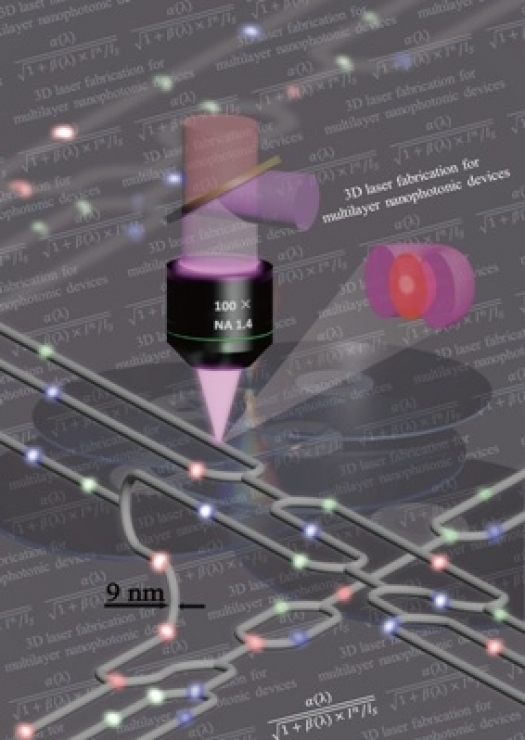
The team has developed a breakthrough technique that enables three-dimensional optical beam lithography at nine nanometres (nm). (The head of a pin is one million nm.)
The technique overcomes a fundamental law discovered in 1873 by German scientist Ernst Abbe.
He determined that a light beam focused by a lens cannot produce a focal spot smaller than half of the wavelength or 500 nm for visible light.
This law enabled the development of modern optical microscopy, an indispensable tool in physics, chemistry, material science and biological science.
However, this fundamental law also set up a barrier for scientists to access small structures on the nanometre scale.
"Optical beam lithography is the ultimate approach to 3D nanofabrication," Gu says.
"However, the diffraction nature of light prevents us from achieving nanometre resolution in a single-beam optical beam lithography system."
Gu explains by using a second donut-shaped beam to inhibit the photopolymerisation triggered by the writing beam in the donut ring, two-beam optical beam lithography can break the limit defined by the diffraction spot size of the two focused beams.
He adds that the key to 3D deep sub-diffraction optical beam lithography was the development with CSIRO of a unique two-photon absorption resin.
"This enabled a two-channel chemical reaction associated with the polymerisation and its counterpart of inhibited polymerisation, respectively, which eventually attributed to build mechanically robust nanostructures. Thus, the development of the vertical integration of integrated circuits, leading to ultra-fast optical information signal processors, becomes possible in the near future," Gu continues.
This is a goal of the Centre for Excellence for Ultrahigh-bandwidth Devices for Optical Systems, funded by the Australian Research Council.
"Worldwide generated information doubles every two years. This breakthrough could lead to reduced cost and reduced energy consumption in data storage," Gu concludes.
This research has been published in the online in the paper, Three-dimensional deep sub-diffraction optical beam lithography with 9"‰nm feature size," by Zongsong Gan et al in Nature Communications, 4, Article number: 2061. doi:10.1038/ncomms3061


