
Omron mass producing probe pin for IC inspection
The firm says its electroforming technology enables finer pitches
Japanese firm Omron Corporation has developed an ultra-compact probe pin electroformed through an electroplating process, and commenced its mass production.
A probe pin is a contact pin used for inspection of electronic components. The employment of electroforming technology has led to superior characteristics, which are difficult to achieve with the currently available cutting process.
In particular, Omron's new probe pin enables a very fine pitch, versatile contact shapes, and a multiple contact point configuration, while being capable of handling a high current load.
Development Background
In recent years, packaging density has been increasing for SMT ICs, LCDs, fine-pitch glass substrates, and other electronic components. This has allowed such components to incorporate more and more sophisticated functions in electronic equipment.
At the same time, these electronic components have a very large number of pins and electrode pads, and they are laid out very close to each other on a PCB. Inspection of electronic components uses a probe pin. Such high-density devices require inspection of many areas, so multiple probe pins must be placed with a very small spacing between each.
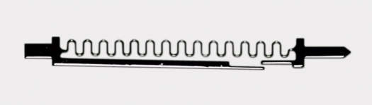
A probe pin typically has a cylindrical shape and consists of multiple parts, namely plungers (contacts), a coil spring, and a barrel to house them. Due to this configuration, the conventional probe pin has several drawbacks, which make it difficult to meet a customer's requirements for fine-pitch, multi-point inspection.
These drawbacks include:
- Limitations as to how far a probe pin's diameter can be reduced using the conventional cutting process, which makes it difficult to support finer pitches.
- Because the probe pin consists of multiple parts, the conduction path becomes complex, thus making contact resistance unstable.
- Making the spring's coil diameter smaller increases conductor resistance, causing heat generation and the spring's disconnection.
Omron overcame these problems by creating a new structure using the company's proprietary electroforming technology. The result is an electroformed probe pin that has a structure entirely different from that of a conventional probe pin.
Features
1. Flat structure makes it easier to reduce pitch
With a conventional probe pin with a cylindrical structure, the molding of a thinner socket becomes extremely difficult in the case of a fine pitch. Omron's electroformed probe pin employs a flat structure, which enables placement of pins at any angle, thus making it easier to reduce pitch compared to a conventional cylindrical probe pin. It is also possible to use a general cylindrical socket housing with the flat probe pin.
2. High-precision formation of versatile shapes enables creation of separate spring and barrel sections in a single component
Omron's proprietary, advanced electroforming technology capable of forming versatile shapes enables a single component to incorporate a spring section to provide contact force and durability, and a barrel section that turns on power when it fits the plunger, separate from each other. No electricity flows through the miniaturized spring section, thus solving such problems as excessive temperature rise, the spring section's disconnection, and unstable resistance.
3. Quick delivery of customised products is possible as no die is necessary
Omron's electroforming technology eliminates the necessity for costly investment in press dies and other equipment, as well as the time-consuming die-making process for prototyping and mass production of probe pins. Specific demand for customized non-standard specifications can be satisfied speedily.
4. Other benefits brought about by OMRON's electroforming technology:
Omron's probe pin provides a smooth contact end surface that protects objects to be inspected from damage. It can also have multiple miniaturised contacts, and offers high durability through the use of OMRON's original material.
Applications
A contact pin for inspection of semiconductors, glass substrates, LCDs, PCBs, etc.
Contact resistance: 100mΩ max. pin (at DC20mV max., 100mA max.)
Contact force: 15gf
Mechanical durability: 500,000 times
Price : Open
Sales Target: 5,000,000 pins/month
Terminal Shape Formation through Electroforming Technology
Electroforming is a metal forming process that forms ultra-thin metal components through the electroplating process. The components are produced by developing a layer of metal onto a base form (master).
Once the plated layer has been built up to the desired thickness, this newly formed part is stripped off the master substrate. Electroforming enables high-precision production of extremely small, thin and fine parts. OMRON also produces dies using microfabrication technology to meet more exacting needs for shapes and sizes, thus enabling transfer of a pattern with submicron-scale (0.0001mm) accuracy.
Omron's small battery connector using subminiature electroformed contacts now employed for smartphones
In December of 2012, OMRON developed a battery connector with a pitch of 2mm and a depth of 2.6mm, using subminiature contacts. The firm's electroforming technology made it possible to produce these contacts that are impossible to form with conventional press technology.
Omron says its battery connector can reduce the footprint on PCBs of smartphones, mobile phones, and other mobile devices, thus contributing to further miniaturization of devices and larger battery sizes.


