
News Article
EVG develops room-temperature wafer debonding platform
The firm's three high-volume-production room-temperature debonding process types are supported by a supply chain of seven qualified adhesive suppliers to enable greater manufacturing flexibility
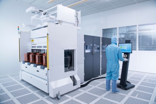
EV Group (EVG), a supplier of wafer bonding and lithography equipment for the MEMS, nanotechnology and semiconductor markets, has unveiled its "LowTemp" debonding platform,. This features three different room-temperature wafer-debonding processes and an extended material supply chain. The platform includes two new debonding processes that have been qualified for EVG's high-volume production temporary bonding/debonding (TB/DB) systems-UV laser debonding and multilayer adhesive debonding-in addition to EVG's ZoneBOND technology. ZoneBOND has already been implemented into production across the advanced packaging and compound semiconductor markets. EVG's LowTemp debonding platform is complemented by a supply chain of seven material suppliers, with a wide choice of qualified adhesives that support a variety of bonding applications and offer greater process flexibility for customers. The LowTemp room-temperature debonding platform is available on the company's temporary bonding/debonding systems, including the recently developed EVG850TB/DB XT Frame platform. "For more than 15 years, EVG has provided leading-edge temporary bonding and debonding solutions to our customers," comments Paul Lindner, EVG's executive technology director. "The experience and know-how that we've built up from our numerous installations in high-volume manufacturing has taught us that one solution doesn't fit all applications when it comes to temporary bonding/debonding." Lindner continues, "Accordingly, EVG offers highly flexible and modular equipment, a wide choice of qualified materials to support customers' individual requirements and multiple source policies, and process development and implementation support through our worldwide application labs and cleanroom infrastructure across a range of applications-including interposers, stacked memory, memory on logic, power devices and compound semiconductors." The LowTemp debonding platform is available on EVG's full line-up of TB/DB systems, including the EVG850TB/DB XT Frame high-volume production platform, which can achieve a throughput of more than 40 wafer stacks per hour. It features an optional, integrated in-line metrology module that takes up to 300,000 measurement points at unprecedented speeds to enable real-time monitoring of the bonding/debonding process for maximum yields.


