
News Article
Silicon not cast out for ARPA-E power device funding
Although the majority of the $25 million funding for power devices will probably be used for wide band gap compound semiconductors gallium nitride (GaN) and silicon carbide (SiC), innovations could also make silicon a contender
The Department of Energy's Advanced Research Projects Agency "“ Energy (ARPA-E) has issued two new Funding Opportunity Announcements (FOAs) for high-current wide bandgap (WBG) power semiconductor devices.
1(a) Dominant GaN device architecture today, the HEMT heterostructure
1(b) Vertical GaN device architecture
However, the lateral GaN HEMT device architecture has two key limitations. Firstly, substantial gate/drain lateral spacing must be maintained to allow for high breakdown voltages. This requirement substantially reduces the effective current density (relative to die size) that can be achieved in these devices and also leads to a reduction in effective current density as breakdown voltage is increased. Low current densities drive down the number of die that can be fabricated on each wafer as voltage ratings increase, thus increasing the cost for a given amperage rating. Secondly, thermal management is complicated by the fact that all current flow is confined to a relatively thin portion of the device near the top surface. Joule heating related to device losses must be dissipated across the thickness of the substrate, motivating research into advanced wafer thinning or complicated thermal spreading approaches to device assembly. In contrast, vertical GaN device architectures as illustrated in Figure 1(b), could overcome these limitations. Such device architectures for GaN power semiconductor transistors, could substantially reduce cost and increase current densities (relative to die size). Vertical device structures for GaN have, thus far, received relatively little attention in the research community but have been recognised as a necessary eventual device architecture for use in high power automotive applications. As with vertical FET and IGBT technologies in silicon, it is expected that vertical devices will be able to achieve higher effective current densities and will enable improved thermal management. Recent demonstrations of high-voltage vertical structure GaN devices appear very promising.
Description of transformational and disruptive technologies in terms of cost, performance, and scale. ARPA-E supports research that establishes new learning curves. A transformational technology becomes disruptive after passing the tipping point The deadline to submit a Notice of Intent for a SWITCHES FOA is 5 p.m. ET on July 8th, 2013. Full applications are due by 5 p.m. ET on July 19th, 2013. Additional information on SWITCHES FOAs can be found on ARPA-E's online application portal, ARPA-E eXCHANGE. ARPA-E strongly encourages outstanding scientists and engineers from different organizations, scientific disciplines, and technology sectors to form new project teams for SWITCHES. ARPA-E has published a list of potential teaming partners for the SWITCHES FOAs on ARPA-E eXCHANGE. Any organisation that would like to be included in this list should visit https://arpa-e-foa.energy.gov/Applicantprofile.aspx and complete all required fields.
The projects will concentrate on improving performance and the cost for power devices.
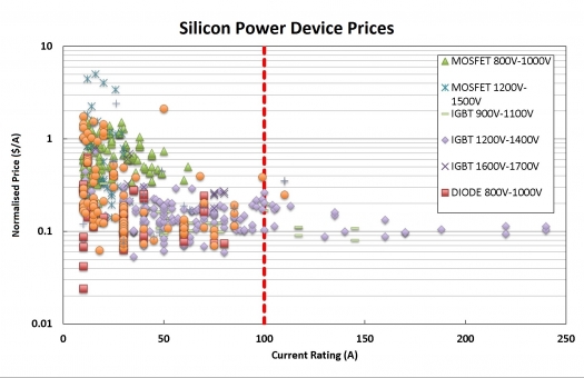
The FOAs are called "Strategies for Wide Bandgap, Inexpensive Transistors for Controlling High Efficiency Systems (SWITCHES)." Both FOAs seek to fund innovative WBG semiconductor materials, device architectures, and device fabrication processes that promise to enable increased energy density, increased switching frequencies, enhanced temperature control, and reduced power losses in a range of power electronics applications, including high-power electric motor drives and automotive traction drive inverters. ARPA-E is allocating up to $25 million for both SWITCHES FOAs, with $15 million in funding being made available to small businesses under ARPA-E's Small Business Innovation Research (SBIR) and Small Business Technology Transfer (STTR) program and $10 million being made available to all applicants Traditionally, silicon devices dominated the power device market. A graph showing normalised silicon power device prices is shown at the top of this story and shows the progressive reduction in cost according to device type. But as this material has several important limitations, silicon is now having to compete with wide bandgap semiconductors in the form of silicon carbide (SiC) and gallium nitride (GaN).Advantages of SiC and GaN over silicon
1(a) Dominant GaN device architecture today, the HEMT heterostructure
1(b) Vertical GaN device architecture
However, the lateral GaN HEMT device architecture has two key limitations. Firstly, substantial gate/drain lateral spacing must be maintained to allow for high breakdown voltages. This requirement substantially reduces the effective current density (relative to die size) that can be achieved in these devices and also leads to a reduction in effective current density as breakdown voltage is increased. Low current densities drive down the number of die that can be fabricated on each wafer as voltage ratings increase, thus increasing the cost for a given amperage rating. Secondly, thermal management is complicated by the fact that all current flow is confined to a relatively thin portion of the device near the top surface. Joule heating related to device losses must be dissipated across the thickness of the substrate, motivating research into advanced wafer thinning or complicated thermal spreading approaches to device assembly. In contrast, vertical GaN device architectures as illustrated in Figure 1(b), could overcome these limitations. Such device architectures for GaN power semiconductor transistors, could substantially reduce cost and increase current densities (relative to die size). Vertical device structures for GaN have, thus far, received relatively little attention in the research community but have been recognised as a necessary eventual device architecture for use in high power automotive applications. As with vertical FET and IGBT technologies in silicon, it is expected that vertical devices will be able to achieve higher effective current densities and will enable improved thermal management. Recent demonstrations of high-voltage vertical structure GaN devices appear very promising.
ARPA-E FOA funding considerations
Description of transformational and disruptive technologies in terms of cost, performance, and scale. ARPA-E supports research that establishes new learning curves. A transformational technology becomes disruptive after passing the tipping point The deadline to submit a Notice of Intent for a SWITCHES FOA is 5 p.m. ET on July 8th, 2013. Full applications are due by 5 p.m. ET on July 19th, 2013. Additional information on SWITCHES FOAs can be found on ARPA-E's online application portal, ARPA-E eXCHANGE. ARPA-E strongly encourages outstanding scientists and engineers from different organizations, scientific disciplines, and technology sectors to form new project teams for SWITCHES. ARPA-E has published a list of potential teaming partners for the SWITCHES FOAs on ARPA-E eXCHANGE. Any organisation that would like to be included in this list should visit https://arpa-e-foa.energy.gov/Applicantprofile.aspx and complete all required fields.


