
News Article
Yole: MEMS expertise to aid IR detector market
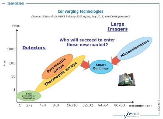
The market analyst says that the next growth opportunities outside traditional IR detector markets are smart building automation and mobile phones. And companies such as Omron and Panasonic have used their MEMS technological know-how to dominate thermopile technology in the array detector market
According to Yole Développement's report, "Infrared Detectors Technology & Market Trends," the total infrared detector market generated revenue of more than $153 million in 2012. This was mostly due to the mature motion detection market which relies on high-volume sales of automatic lighting and intrusion detection systems. However in a scenario that includes spot thermometer function in mobile devices, it is expected that these revenues will top at as much as $381 million in 2018, growing at a 16 percent CAGR. This will be fuelled by small detector applications and medium to large array detectors. The main small detector applications will be dominated by consumer mobile applications. The growth in mobile applications is expected to be driven, in the short term, by adoption of monopixel sensors for internal temperature measurement and spot thermometry in smartphones and tablets. Technological innovation will be the key to compete successfully with other processes in that market. Wafer-level-packaging will be necessary to successfully address these markets driven by price and looking for ever smaller form factor sensors. A specific scenario for adoption of IR sensors in mobile devices is anticipated to raise market revenues in 2018 by $30 million. Medium size array detectors range from (4 x 4) to (16 x 16) pixels, while the large size is represented by (32 x 32) pixels and above. Yole expects these to grow at a CAGR of around 30 percent in the 2013 to 2018 period. Medium size arrays have started to be successfully sold in HVAC for buildings and automotive, people counting for retail, home appliances and will continue to expand due to affordable pricing. Large size arrays are expected to target the key market for smart building automation that will use a wide variety of detector functions and could support higher pricing. However, overall, these positive market dynamics will be fuelled by detector price erosion. Historically, technological evolution has pushed IR detectors toward higher-end markets with array detectors. Low cost and easy to manufacture, IR detectors have been used in a wide diversity of markets such as construction, security, appliances, and industrial, and for a wide variety of functions, for example, in motion detection, temperature measurement, counting and fire & gas detection. Initially limited to single pixel pyroelectric detectors with a basic motion detection function, IR detectors have progressively been used in more complex systems which diversified the market into higher-end applications such as temperature sensing, or gas & fire detection and spectroscopy. At the end of 2000, that diversification was pushed further into the high end of the market by the introduction of array detectors. Multiple companies, led by Heimann Sensors, adopted a "technology push" strategy to introduce IR detector arrays either based on pyroelectric technology or thermopile technology. Coming from the MEMS industry, several companies like Omron and Panasonic have ensured the domination of thermopile technology on the array detector market by capitalising on their know-how in complex MEMS structure manufacturing. However, in 2013 the domination of thermopiles has been challenged by a new entrant based on a technology coming from the infrared imaging market: ULIS (Ultimate Integration of Silicon). The very large IR detector is the first microbolometer having a true resolution (without windowing) below 100 x 100 pixels, which aims to gain market share in the developing large IR detector market. A bolometer measures the power of incident electromagnetic radiation via the heating of a material with a temperature-dependent electrical resistance. A microbolometer is a specific type of bolometer used as a detector in a thermal camera. Infrared radiation with wavelengths between 7.5-14 μm strikes the detector material, heating it, and thus changing its electrical resistance. The change in resistance is converted into temperatures which can be used to create an image. Unlike other types of infrared detecting equipment, microbolometers do not require cooling. "In 2014, competition in the small microbolometer array segment is expected to increase with FLIR, the market leader of uncooled infrared imaging. In the future, it is expected that the next technological step for IR detectors will be at the packaging level with either vacuum package or Wafer-Level Package, and at pixel level with manufacturing process optimisation to decrease pixel pitch," says Paul Danini, Technology and Market Analyst, Imaging Technologies & MEMS Devices, at Yole Développement. Major technological barriers prevent current players from moving from low-end to high-end applications. The infrared detector competitive landscape is complex due to the diversity of players in that market. Having a clear understanding of each player's technological background and positioning clarifies what is the total available market and the challenges that will have to be faced. While the small IR detector market is a commodity market driven by price, medium and large array detectors are cost/performance driven and still offer room for differentiation for new entrants. However strong barriers lie between each of the three IR detector technologies, which are pyroelectric, thermopiles and microbolometers. This is because these technologies are based on different manufacturing processes, and making the move from one technology to another is very difficult without a merger or acquisition. Similarly, from a product standpoint, the move from small detectors to array detectors is challenging because it relies on strong IP or on MEMS manufacturing capacities. In this context, many companies are not in direct competition and there is still opportunity to take position in the high-potential large detector market.


