
News Article
Nikon to bag order for 450mm scanner for G450
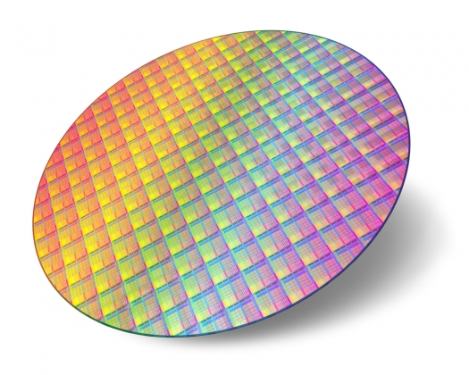
Nikon Corporation has entered into a contract with the Research Foundation for the State University of New York (Research Foundation for SUNY). The firm will provide a 450mm wafer ArF immersion scanner for process development and is to be entrusted with wafer patterning straight after receiving an order for the system. The tool is scheduled to be shipped in April 2015. This 450mm wafer ArF immersion scanner will be used by the member companies of the Global 450 Consortium (G450C) headquartered in the College of Nanoscale Science and Engineering (CNSE) for process development, characterization and demonstrations. Nikon will provide lithography solutions by sending its engineers to G450C. Nikon aims for the standardisation of 450mm wafer ArF immersion scanners by offering early opportunities to develop the 450mm process. Announced by New York Governor Andrew M. Cuomo in September 2011 and located in the Albany NanoTech Complex at CNSE, G450C is a joint effort by five of the biggest computer chip technology companies, Intel, IBM, GLOBALFOUNDRIES, TSMC and Samsung. The goal of G450C is to support the industry transition from 300mm to the 450mm wafer platform, a crucial tipping point for the semiconductor manufacturing process, as smooth as possible. G450C plans to build state-of-the-art infrastructure in the Albany NanoTech Complex to demonstrate the capabilities of 450mm wafer platform and process. The closure of this contract followed the recent orders Nikon has received from a major device manufacturer for the 450mm ArF immersion scanners. Nikon believes this is a result of its development program having won the approval and confidence of the industry. The company expects to see increased orders for its systems from other device manufacturers in time for shipments of high volume manufacturing systems scheduled in 2017.


