
Dow Corning & imec to advance 3D IC packaging
Dow Corning is one of the newest member organisations to join imec, a leading research centre for the advancement of nano-electronics.
The announcement signals expanded opportunities for both organisations to combine their expertise toward the development and broader adoption of 3D integrated circuit (IC) packaging technologies, wherein IC chips are stacked in vertical 3D architectures.
"This move is a natural and strategic step for Dow Corning and imec, as we both believe collaborative innovation is as critical to industry leadership as native expertise," says Andrew Ho, global industry director, Advanced Semiconductor Materials at Dow Corning.
"Our access to imec's world-class resources and expertise will not only help us further refine our unique temporary bonding solution, it will allow imec to leverage that solution to advance integration of the 3D IC packaging process that they've been developing for years," adds Ho.
By integrating multiple chips into a single package, 3D IC technology promises to reduce form factor and power consumption, and increase bandwidth to enable more efficient inter-chip communication for next-generation microelectronics devices. Yet, before 3D IC fabrication can see broader adoption, it will require innovative advances in materials and processing technologies.
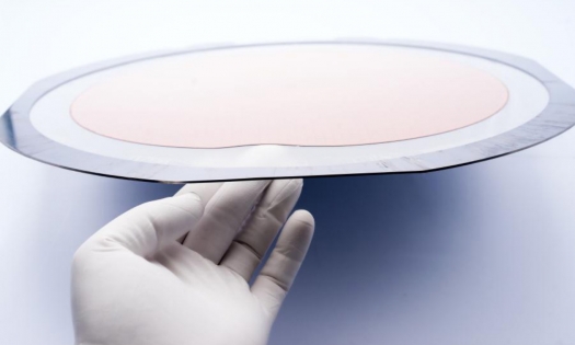
The photo above shows a thin silicon wafer on dicing frame after successful debonding from a silicon carrier wafer at imec, using Dow Corning's silicone-based temporary bonding solution.
One of the key challenges imec is tackling is the bonding of the device wafer to a carrier wafer, prior to wafer thinning, and the safe debonding of the thin wafer after completion of backside processing. This was Dow Corning's goal when designing its Temporary Bonding Solution, aims at simple processing using a bi-layer concept comprising an adhesive and release layer.
The technology also enables room-temperature bonding and debonding processes based on standard manufacturing methods. Together with imec, Dow Corning will explore its temporary bonding CMOS-compatible solution for 3D Through-Silicon-Via (TSV) semiconductor packaging. The collaboration will aim to further expand the technology's ability to achieve simple, cost-effective bonding-debonding techniques compatible with standard manufacturing processes.
"Imec's precompetitive programs are an essential platform for industry leaders to share the risk and cost of advanced research. As one of the semiconductor industry's most proven pioneers in advanced silicone-based solutions, Dow Corning brings valuable materials and processing expertise to imec's global network of innovators "“ as well as a key enabling technology for TSV fabrication," says Eric Beyne, program director 3D System Integration at imec.
"We look forward to collaborating closely with our newest member organization as we drive the next stage of 3D integration, and help ensure compatiblity of the proposed thin wafer carrier solution with advanced, sub-10-nanometer CMOS device technologies," adds Beyne.
Imec will showcase its latest developments at SEMICON West, taking place between July 9th and 11th, 2013 at booth # 1741, South Hall.


