
News Article
KLA-Tencor defect analysis on another level
Coupling electron-beam review with optical inspection facilitates rapid defect discovery, identification and sourcing
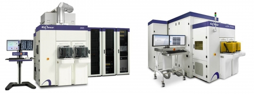
KLA-Tencor Corporation has revealed the new 2910 Series optical wafer defect inspection platform with NanoPoint technology and the new eDR-7100 electron-beam wafer defect review system. Meeting IC manufacturers' need for accelerated defect sourcing on advanced devices, these two tools combine increased speed with seamless connectivity to quickly find and identify defects that inhibit yield and reliability. The 2910 Series' improved defect capture and the eDR-7100's enhanced review resolution have been demonstrated by detecting and imaging unique defects located at the bottom of three-dimensional or vertical pattern structures such as FinFETs. "Our customers' need to quickly ramp processes that use complex patterning strategies creates defect challenges that drive our ongoing innovation in both optical and electron-beam technologies," says Bobby Bell, executive vice president of KLA-Tencor's Wafer Inspection Group. "We continue to extend optical inspection through novel methods such as our NanoPoint technologies. These advances take our 2910 Series tools to a new level of optical defect detection while preserving optical inspection speed. Additional developments in e-beam technology allow our eDR-7100 to accurately identify extremely tiny defects that are not always visible on other e-beam review tools. Pairing these tools provides our customers with an efficient inspection and review solution for qualifying their leading-edge processes." Building on the defect discovery capabilities produced by KLA-Tencor's patented NanoPoint technologies, the 2910 Series features new optical apertures and inspection modes that have been shown to provide a substantial improvement in the capture of several yield-critical defect types, such as voids, bridges and bottom bridges. What's more, the tools feature a significant increase in throughput over the previous-generation 2900 Series, enabling engineers to sample more wafers or inspect additional process levels for faster identification of yield excursions. The eDR-7100 includes fourth-generation e-beam immersion optics, producing improved resolution and additional review modes for imaging a wide range of defect types, with a particular benefit being the tool's ability to locate and identify defects at the bottom of complex pattern features or high-aspect ratio structures. These technical advances also enable enhanced throughput compared to the eDR-7000, allowing engineers to sample additional defects to gain a more accurate understanding of the defect population on the wafer. Since IC fabs increasingly require e-beam review of unpatterned wafer defects detected by inspectors such as the Surfscan SP3, the eDR-7100 features a new optical microscope and energy-dispersive x-ray (EDX) compositional analysis subsystem to aid in the classification and characterization of bare wafer defects. Multiple 2910 Series optical inspection tools, configured as either the 2910 or 2915, and eDR-7100 e-beam review tools have been installed at leading IC manufacturers where they are being used for new technology development and ramp. In order to help protect a fab's capital investment, the 2910 Series and the eDR-7100 tools are both upgradeable from their predecessors, the 2900 Series and the eDR-7000, respectively. To maintain the high performance and productivity demanded by leading-edge production, the 2910 Series and eDR-7100 tools are backed by KLA-Tencor's global, comprehensive service network.


