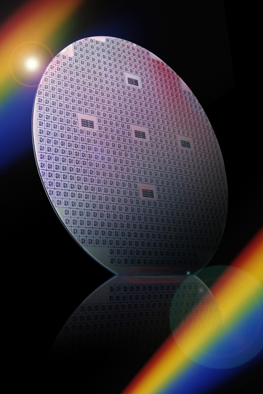
PCB technology company Rainbow Technology Systems has developed a unique coating system for photo tools which addresses a key issue that costs the electronics industry thousands of pounds each day.
Traditional methods of printing solder masks use photo tools to lay the pattern on the PCB (printed circuit board). However, there are frequently issues with scaling due to the effect of heat, movement and humidity on the photo mask.
Often three or four iterations of photo tool need to be produced to get the right fit. Not only is this time consuming but it is also very costly in terms of throwing away expensive materials. Sticking occurs which means that very often after a small number of uses the phototool is no longer serviceable, and cleaning exacerbates the problems.
Rainbow's Panda Coater applies a thin protective coating to the photo tool which makes it hydrophobic, chemically resistant and scratch resistant. This means that only one photo tool is required, as scaling is not affected by environmental factors or movement. The coating can also extend the usable life of the photo tool by up to ten times making it ideal for high-volume production.

Panda Coater
The Panda Coater offers many advantages over conventional methods of coating. Its patented Smart Coating Dispenser system ensures that only the optimal amount of coating fluid is used to coat the material. Conventional "roller in bath" systems can be extremely wasteful, expensive to run and messy.
A thin, transparent, scratch and chemically resistant coating, typically 4 microns, is applied to the substrate. It then passes through the integrated, controlled environment UV curing tunnel and is ready for immediate use. Both thick and thin calibre materials can be processed and the unit automatically senses the exact size of the sheet so only the required amount of liquid is dispensed.
At the front end of the unit is an integrated Teknek contact cleaning unit which ensures the material is completely free of any contamination (particles down to one micron) before being processed.
Other key features of the Panda Unit include:
· Circulating coating fluid is gently agitated to ensure a homogenous mix
· Small footprint "“ 1m x 1.2m
· Accommodates material widths up to 660mm
· Easy access for maintenance and cleaning
· Rapid start up and low energy consumption
· Small fluid reservoir (5 litres) means easier and cleaner maintenance
· Clean-room compatible paint finish
"Our goal at Rainbow is to find solutions for the electronics production sector which are practical, cost-effective and good for the environment," says Jonathan Kennett, CEO of Rainbow Technology Systems. "The Panda Coater represents a breakthrough in coating technology and addresses a key issue for the industry - how to stabilise photo tools - saving substantial amounts of time and money in high volume manufacturing."
Rainbow Technology Systems was established in 2005 to develop fine line printing technologies for the PCB market. In 2012 the company launched the revolutionary Rainbow Process Unit which represents a breakthrough for the electronics industry by incorporating coating, imaging and developing of PCBs in one compact, automated unit which promises to make board production faster, easier and more profitable.
The completely self-contained unit takes up only 12 square metres of floor space and does not require a clean room environment. The process is automatic requiring minimal operator intervention and is capable of delivering a double sided panel every 20 seconds ready for etching.
Key to the success of the Rainbow Process is the proprietary etch wet resist which does not require pre-drying (using a curing oven) before imaging. The resist is 100 percent solids and solvent free.
Using only UV LEDs and standard photo-tools tracks and gaps of 20 microns and below are easily achieved. The unit has very low running costs with power consumption averaging 3kW.
The technology behind the Rainbow Process is the brainchild of chief executive and founder Jonathan Kennett. Kennett pioneered the development of contact cleaning technology for the electronics and high-tech sectors 25 years ago when he founded Teknek which has become one of the global leaders in contact cleaning and yield improvement equipment.


