
Revolutionising consumer electronics with nanotechnology
Nanopatterning, or self-assembling molecular materials, form an organised lithographic pattern on semiconductor crystals, for use as integrated circuits. Now newly developed materials, when integrated into electronics, will enable the development of ultra-lightweight, compact and efficient devices
University of Akron (UA) researchers have developed new materials that function on the nanoscale, which could lead to the creation of lighter laptops, slimmer televisions and crisper smartphone visual displays.
Known as "giant surfactants" - or surface films and liquid solutions - the researchers, led by Stephen Z.D. Cheng, dean of UA's College of Polymer Science and Polymer Engineering, used a technique known as nanopatterning to combine functioning molecular nanoparticles with polymers to build these novel materials.
Surfactants are compounds that lower the surface tension (or interfacial tension) between two liquids or between a liquid and a solid. Surfactants may act in a number of ways - as detergents, wetting agents, emulsifiers, foaming agents, or dispersants, to name a few.

Stephen Cheng
The giant surfactants developed at UA are large, similar to macromolecules, yet they function like molecular surfactants on a nanoscale, Cheng says.
The outcome?
Nanostructures that guide the size of electronic products.
Nanopatterning, or self-assembling molecular materials, is the genius behind the small, light and fast world of modern-day gadgetry, and now it has advanced one giant step thanks to the UA researchers who say these new materials, when integrated into electronics, will enable the development of ultra-lightweight, compact and efficient devices because of their unique structures.
During their self-assembly, molecules form an organised lithographic pattern on semiconductor crystals, for use as integrated circuits. Cheng explains that these self-assembling materials differ from common block copolymers (a portion of a macromolecule, comprising many units, that has at least one feature which is not present in the adjacent portions) because they organise themselves in a controllable manner at the molecular level.
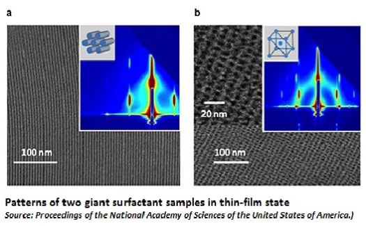
Patterns of two giant surfactant samples in thin-film state are shown at the top of this story.
"The IT industry wants microchips that are as small as possible so that they can manufacture smaller and faster devices," says Cheng, who also serves as the R.C. Musson and Trustees Professor of Polymer Science at UA.
He points out that the current technique can produce the spacing of 22 nm only, and cannot go down to the 10 nm or less necessary to create tiny, yet mighty, devices. The giant surfactants, however, can dictate smaller-scale electronic components.
"This is exactly what we are pursuing - self-assembling materials that organize at smaller sizes, say, less than 20 or even 10 nanometres," says Cheng, equating 20 nm to 1 /4,000th the diameter of a human hair.
Team's work has commercial applications
An international team of experts from UA, Peking University in China, National Tsinghua University in Taiwan and McMaster University in Canada have shown how well-ordered nanostructures in various states, such as in thin films and in solution, offer extensive applications in nanotechnology.
"These results are not only of pure scientific interest to the narrow group of scientists, but also important to a broad range of industry people," says Cheng, noting that his team is testing real-world applications in nanopatterning technologies and hope to see commercialisation in the future.
The team's study is highlighted in a pending patent application through the University of Akron Research Foundation and the article, "Giant surfactants provide a versatile platform for sub-10-nm nanostructure engineering" by Xinfei Yu et al, published in Proceedings of the National Academy of Sciences of the United States of America, 110, 10078-10083, 2013.


