
Cobham simulation takes sputtering a leap forward
The firm's process-wide sputtering simulator improves thin-film deposition efficiency and reduces costs
Cobham Technical Services has launched the first comprehensive simulation solution for designing magnetron sputter coaters.
Sputter coating is widely used for fabricating thin film coatings in a diverse range of applications including semiconductor fabrication, and engineering coatings on products used in some of today's most demanding high technology applications.
The new software tool provides precision simulation of the complete sputtering process, offering a highly practical means of improving sputter target utilisation, plasma formation and thin film deposition.
Cobham believes the new software has the potential to save hundreds of millions of dollars a year in this industry segment because of the costs of the high purity materials required in surface coating applications. The latest application design option is part of the company's Opera finite element analysis multi-physics suite for electromagnetic design.
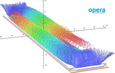
The new Magnetron Sputter version of Opera provides a complete suite of three-dimensional (3D) tools for the finite element modelling, simulation, analysis and optimisation of magnetron sputtering equipment. This is a development that draws on Cobham's two decades of simulation expertise and validation in the field of charged particle beams.
The new software has been validated prior to release in cooperation with two commercial sputter coating companies: Teer Coatings (Miba Coating Group) and Colorado Concept Coatings, and by thin film experts from Thin Film Consulting, and predicts sputter target utilisation to within two percent of actual measured results.
"Industry spends several billion dollars a year on sputtering target material, and it is typical that less than half of each target is used before replacement," says Kevin Ward of Cobham Technical Services. "Increasing target utilisation alone by just a few percent could save hundreds of millions of dollars annually, without considering the other gains that can be achieved by design optimisation such as improved deposition quality and deposition rates, and reduced equipment downtime for target changeovers."
Of the many different types of sputtering processes, magnetron sputtering - where sputtered atoms are ejected from a target by the impact of ions produced within a magnetically confined plasma - offers advantages that have made it a popular choice. Among these are its relatively high sputtering efficiency, and the flexibility to vary the properties of the plasma to control the characteristics of the deposited film.
Sputtering applications all share a need for optimising the deposition profile and quality of film, maximising utilisation of sputter target materials, and minimising processing time. Many variables determine the performance of a sputter coater and the quality of the deposited films, but engineers have had few advanced tools to assist in design and optimisation.
If design software is used, it tends to be for analysing magnetic fields alone, which provides only a partial solution to an overall problem that also involves electric fields and the influence of the plasma. The typical design process for sputtering tools still relies greatly on the construction and test of physical prototypes. This experimental approach makes exploring a broad range of possible design options both costly and time consuming.
For the first time, the complete magnetron sputtering design task can now be performed effectively and efficiently by simulation within pragmatic timescales. The virtual prototyping capability offered by Cobham's new Opera software allows engineers to investigate a wide range of designs and operating regimes in a fraction of the time of an experimental program, and at a fraction of the cost, enabling the optimisation of full lifecycle costs from the outset.
The high fidelity of the Opera finite element simulation tool allows the engineers to rapidly evaluate and optimise detailed characteristics of the sputtering process such as deposited film thickness distribution, erosion groove profile, and sputter target utilisation.
Opera models can include all significant physical processes in a simulation, and parameters can be varied at will to explore the design space thoroughly before producing a physical prototype. In addition to user-directed exploration of any design space, Opera also includes a powerful optimiser tool that performs automatic multi-variable, multi-objective optimisation. Users have the freedom to define objectives - any quantity or combination of quantities that can be calculated in the tool's post-processor can be used - from simple field values to more complex derived quantities such as deposited film profile and target utilisation.
The flexibility of the modelling system and the Opera design tool-chain allows any and all styles of magnetron - such as circular, rectangular, balanced or unbalanced - to be investigated and optimised. The computing efficiency of Opera also allows the analysis of multi-target coaters, where the additional complication of stray fields may be investigated and their effects mitigated through design iteration.
Cobham Technical Services is supporting the launch of the new magnetron sputtering design software with specialist training in the use of the Opera tool and finite element design.


