+44 (0)24 7671 8970
More publications     •     Advertise with us     •     Contact us
 
News Article

Toshiba expanding Yokkaichi fab for memory devices

News

The facility will be used to manufacture NAND flash and 3D memories

Tokyo based Toshiba Corporation held a ceremony in readiness for the start of construction of Phase 2 of Fab 5. This is the company's fabrication facility at its Yokkaichi Operations memory production facility in Mie Prefecture.

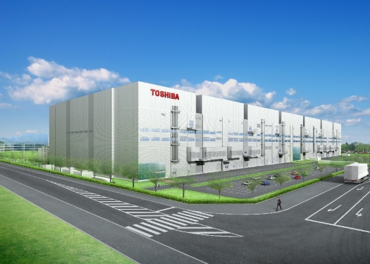
An artist's Impression of Fab 5, Toshiba Yokkaichi Operations is shown at the top of this article.

Toshiba will expand Fab 5 to secure manufacturing space for NAND flash memories fabricated with next generation process technology and for 3D memories. Construction should be completed in summer next year, and decisions on equipment investments and production levels will reflect market trends.

Three fabs at Yokkaichi Operations currently mass produce NAND flash memories, including Fab 5 phase 1. Fab 5's construction was planned around two phases, the first of which went into operation in July 2011.

After considering the balance of product supply and demand, and noting a recovery driven by growing demand for smartphones, tablets, SSD for enterprise servers, Toshiba now anticipates further medium- to long-term market expansion and recognises that the time is right to expand Fab 5.

Going forward, Toshiba will expand business and boost competitiveness by leadership in advanced process technology and the development of new generation memories that answer market needs.


Purdue, imec, Indiana announce partnership
Resilinc partners with SEMI on supply chain resilience
NIO and NXP collaborate on 4D imaging radar deployment
Panasonic Industry digitally transforms with Blue Yonder
Global semiconductor sales decrease 8.7%
MIT engineers “grow” atomically thin transistors on top of computer chips
Keysight joins TSMC Open Innovation Platform 3DFabric Alliance
Leti Innovation Days to explore microelectronics’ transformational role
Quantum expansion
indie launches 'breakthrough' 120 GHz radar transceiver
Wafer fab equipment - facing uncertain times?
Renesas expands focus on India
Neuralink selects Takano Wafer Particle Measurement System
Micron reveals committee members
Avoiding unscheduled downtime in with Preventive Vacuum Service
NFC chip market size to surpass US$ 7.6 billion
Fujifilm breaks ground on new €30 million European expansion
Fraunhofer IIS/EAS selects Achronix embedded FPGAs
Siemens announces certifications for TSMC’s latest processes
EU Chips Act triggers further €7.4bn investment
ASE recognised for excellence by Texas Instruments
Atomera signs license agreement with STMicroelectronics
Gartner forecasts worldwide semiconductor revenue to decline 11% in 2023
CHIPS for America outlines vision for the National Semiconductor Technology Center
TSMC showcases new technology developments
Alphawave Semi showcases 3nm connectivity solutions
Greene Tweed to open new facility in Korea
Infineon enables next-generation automotive E/E architectures
Global AFM market to reach $861.5 million
Cepton expands proprietary chipset
Semtech adds two industry veterans to board of directors
Specialty gas expansion
×
Search the news archive

To close this popup you can press escape or click the close icon.
Logo
×
Logo
×
Register - Step 1

You may choose to subscribe to the Silicon Semiconductor Magazine, the Silicon Semiconductor Newsletter, or both. You may also request additional information if required, before submitting your application.


Please subscribe me to:


You chose the industry type of "Other"

Please enter the industry that you work in: